Highlight: STM banopatterning on pristine Nb-doped SrTiO3 surfaces

Collaborative users from the Advanced Photon Source at the Argonne National Laboratory, working with the Electronic & Magnetic Materials & Devices Group, have found a controllable way to modify the surfaces of pristine Nb-doped SrTiO3 (Nb:STO) at the nanoscale.
For decades, most of the work on noncleavable STO focused on heavily treated surfaces (chemical etching, sputtering/annealing).
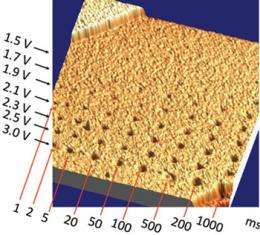
This is the first scanning tunneling microscope (STM) work on how the tip can interact with pristine Nb:STO surfaces created by in situ fracturing. By fracturing Nb:STO at ~50 K, ~500-nm atomically flat TiO2 terraces with a random covering of SrO molecules are attained.
Using a pulsed sample-tip bias, the SrO clusters can be removed and redeposited reversibly from surface to STM tip.
This work demonstrates the interaction between the STM tip and oxide surfaces, and it offers a pathway to creating nanoscale objects on single-crystal oxide surfaces.
More information: T. Chien, T. Santos, M. Bode, N. Guisinger, J. Freeland, Appl. Phys. Lett. 95, 163107 (2009).


