New solder for semiconductors allows good electronic performance

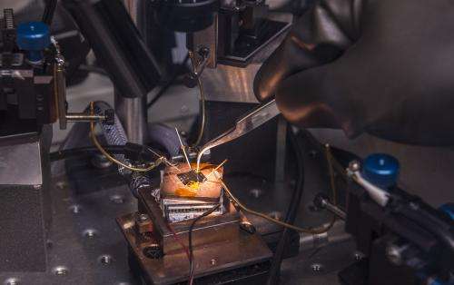
A research team led by the University of Chicago's Dmitri Talapin has demonstrated how semiconductors can be soldered and still deliver good electronic performance.
"We worked out new chemistry for a broad class of compositions relevant to technologically important semiconductors," said Talapin, a professor in chemistry.
Semiconductors sit at the heart of most electronics. From computer chips to solar cells, these materials conduct electricity and make it possible to generate and control electrical current. The compounds that Talapin and his associates have developed can be used to join pieces of semiconductor. Researchers and engineers have long struggled with joining together semiconducting surfaces, which are very sensitive to impurities and structural defects.
"If you put two pieces of semiconductor next to each other, each joint will be unique and in most cases will block transport of charges," Talapin said. "You will not be able to make a reasonably good electronic circuit by simply taking different semiconductor pieces and pressing them against each other as you could do with metals."
Talapin and his associates from UChicago, Argonne National Laboratory, and the Illinois Institute of Technology published their findings in the Jan. 23, 2014, issue of Science. They have developed compounds of cadmium, lead, and bismuth that can be applied as a liquid or paste to join two pieces of a semiconductor by heating them to several hundred degrees Celsius, which is mild by industry standards.
"Our paste or our liquid converts cleanly into a material that will be compositionally matched to the bonded parts, and that required development of new chemistry," Talapin said. "We had to design special molecules that fulfill this requirement so that they do not contaminate the material." After application as a liquid or paste, they decompose to form a seamless joint.
Diverse applications
"Dr. Talapin's work is exciting because its applications are so diverse," said Eric Ginsburg, assistant director at UChicagoTech, the University's Center for Technology Development and Ventures.
"We expect it to be used soon by manufacturers who need to join semiconductor parts, but it could also create new markets in the growing semiconductor industry. For example, it would enable 3-D printing of semiconductors and create possibilities for new technologies."

Ginsburg and Cristianne Frazer, UChicagoTech project manager, have previously helped Talapin to license his technologies. They are working closely with Talapin, industry contacts, and investors to determine a strategy for developing the new solder material.
Use of the U.S. Department of Energy's Advanced Photon Source at Argonne was critical to the project's success.
"The classical, top-down manufacturing process in the silicon industry does not require soldering," Talapin said. Instead, industry engineers make a large silicon crystal, then cut, carve and etch it into the desired shapes.
Semiconductor soldering is unlikely to have a major impact on today's mainstream silicon technology, but could lead to the development of less expensive, solution-processed semiconductors needed for entry into new markets. Among these markets are printable electronics, 3-D printing, flat panel display manufacturing solar cells and thermoelectric heat-to electricity generators for the Internet of Things (IoT).
Printable electronics requires assembly of semiconductors from small pieces, putting tiny grains together like Legos. "It's like what people call additive manufacturing, when you add things and build from pieces," Talapin said. "If you want to assemble pieces, you need a solder or glue or connectors."
3-D printing is an exponentially growing market, Talapin noted. "We can 3-D print, to my knowledge, almost any class of materials, but not semiconductors." His new solder may change that.
A tiny transistor operates each pixel in current-generation flat-screen televisions. These transistors currently are manufactured via vacuum methods, but industry experts expect that to change to printing and other less expensive solution-based manufacturing techniques.
Internet of Things

The Internet of Things is a growing network of everyday objects—traffic lights and cars, for example—that can communicate automatically via miniature web servers. Tiny sensors will be integrated in buildings and bridges to immediately report a crack or other structure failure. Semiconductors will be needed to convert sunlight or heat to electrical currents used to receive, process and transmit information within such a network.
"That requires very inexpensive semiconductors for electronic circuits and devices that come essentially at the price of a postage stamp," Talapin said. Printing electronics in a way similar to printing postage stamps. It is a chemistry problem to find the right "inks" for this purpose, he said. "Right now postcards and magazines are simply colorful, but there's nothing that precludes them from being colorful and electronically active, so that as ink dries it forms a film that can conduct charges. It's not sci-fi these days."
Solar cells also represent an increasingly lucrative, highly competitive, multibillion-dollar annual market, one that fuels the quest for improved solution-process manufacturing methods for semiconductors.

"Solution-processed semiconductors is a huge field. We definitely have hundreds of competitors, both in academic settings and in companies," Talapin said. "It's a very competitive area because it's now on the final approach to big money."
The Science article mentioned in passing that their semiconductor soldering approach set a new record for electron mobility in solution-processed semiconductors, a measure for how quickly electrons move through the materials. The new record is almost 10 times faster than the old one.
"It's mind-blowing," Talapin said.
More information: "Composition-matched molecular 'solders' for semiconductors," by Dmitriy S. Dolzhnikov, Hao Zhang, Jaeyoung Jang, Jae Sung Son, Matthew G. Panthani, Tomohiro Shibata, Soma Chattopadhyay, and Dmitri V. Talapin, Science, Jan. 23, 2015, Vol. 347, No. 6220, pp. 425-428, DOI: 10.1126/science.1260501. First published online Jan. 1, 2015.
Journal information: Science
Provided by University of Chicago


