Bursting through the silicon barrier: Developing carbon-based nanoelectronics with graphene

Nov 27, 2012
Bursting through the silicon barrier: Developing carbon-based nanoelectronics with graphene

(Phys.org)—On the road towards creating smaller and smaller electronic devices, silicon blocks the way by limiting the smallness of the electronic components that can be constructed with it.  A promising way forward has been found by using carbon instead and its study has resulted in a rapidly growing field.  In a work published in ACS Nano, using tools including those found at the Synchrotron Radiation Center, scientists have developed a process for making a never-before-seen, atomically thin, composite material containing ordered layers of graphene and nanocrystals of graphene monoxide.

Graphene, composed of an atomically thin layer of carbon, does not by itself have the necessary properties that lend itself for use in modern .  To achieve this, other elements need to be added to the mix.  When oxygen is added chemically to graphene, for example, a property called the band-gap is created.  The band-gap determines the of a material, an important factor in creating useful electronic devices.  However, at this stage, the mix is a disorganized arrangement of atoms, and results in poor , including the band-gap. Because of this it can only be used in basic electronic devices such as supercapacitors, sensors, and flexible transparent conductive electrodes. 

In this publication researchers describe a method for annealing (heating) the graphene and oxygen mix resulting in a previously unobserved atomic structure.  It is comprised of layers of oxygen poor graphene sandwiched between layers of oxygen rich graphene (graphene oxide). 

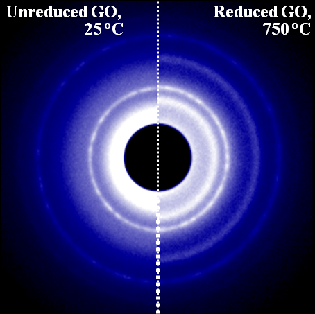
In the image, the number of rings corresponds to the complexity of the different structures in the (G-O) compound.  The left side of the image corresponds to the G-O compound before annealing (heating).  The right side of the image, corresponding to the compound after annealing, shows additional rings indicating a more complex and ordered structure.

Scientists determined that the new carbon based structure shows promise allowing them to tailor it creating, for example, ideal "band gaps" for use in nanoelectronic devices such as sensors, transistors, and optoelectronic devices.

Explore further: Topographical approaches to measuring graphene thickness

More information: pubs.acs.org/doi/abs/10.1021/nn203160n

Related Stories

Two graphene layers may be better than one

Apr 27, 2011

(PhysOrg.com) -- Researchers at the National Institute of Standards and Technology have shown that the electronic properties of two layers of graphene vary on the nanometer scale. The surprising new results ...

Damaging graphene to create a band gap

Nov 22, 2010

(PhysOrg.com) -- "Graphene offers a lot of interesting potential applications for nanoelectronics," Florian Banhart tells PhysOrg.com, "but there is no band gap. This is a well-known problem. Without the band gap, switch ...

Toward a better understanding of bilayer graphene

Oct 26, 2010

(PhysOrg.com) -- "Graphene is a very exciting material with a number of interesting possibilities, including for use in electronic devices," Pablo Jarillo-Herrero tells PhysOrg.com. "However, all graphene system ...

Topographical approaches to measuring graphene thickness

Sep 28, 2012

(Phys.org)—Graphene has long shown potential for use in electronics, but difficulties in producing the material to a high enough quality has so far prevented the commercialisation of graphene-based devices.

Recommended for you

Hybrid material as gold-leaf substitute

Jun 18, 2013

(Phys.org) —A team of researchers headed by Professor Raffaele Mezzenga has created a hybrid material out of gold and milk proteins that looks like a wafer-thin gold leaf. Thanks to its properties, it could ...

Antioxidant with a long shelf life

Jun 17, 2013

(Phys.org) —Scientists from ETH Zurich have developed a nanomaterial that protects other molecules from oxidation. Unlike many such active substances in the past, the ETH-Zurich researchers' antioxidant ...

Fast pollutant degradation by nanosheets

Jun 17, 2013

(Phys.org) —Waste from textile and paint industries often contains organic dyes such as methylene blue as pollutants. Photocatalysis is an efficient means of reducing such pollution, and molybdenum trioxide ...

Unzipped nanotubes unlock potential for batteries

Jun 13, 2013

(Phys.org) —Researchers at Rice University have come up with a new way to boost the efficiency of the ubiquitous lithium ion (LI) battery by employing ribbons of graphene that start as carbon nanotubes.

Nanoparticle opens the door to clean-energy alternatives

Jun 13, 2013

(Phys.org) —Cheaper clean-energy technologies could be made possible thanks to a new discovery. Research team members led by Raymond Schaak, a professor of chemistry at Penn State University, have found ...

User comments : 0

More news stories

Sound waves precisely position nanowires

(Phys.org) —The smaller components become, the more difficult it is to create patterns in an economical and reproducible way, according to an interdisciplinary team of Penn State researchers who, using ...

An environmentally friendly battery made from wood

Taking inspiration from trees, scientists have developed a battery made from a sliver of wood coated with tin that shows promise for becoming a tiny, long-lasting, efficient and environmentally friendly energy ...

Hybrid nanostructures: Getting to the core

Material scientists expect the new multifunctional properties of hybrid nanostructures will transform the development of high-performance devices, including batteries, high-sensitivity sensors and solar cells. ...

Sweet solutions for detecting disease

Based at the Institute of Chemistry in the Slovak Academy of Sciences, Ján Tkáč's research combines glycomics – the study of sugars in organisms – with biochip sensors based on nanoparticles and nanotubes. ...