Ordered nanocrystal arrays may provide a new platform to study and tailor the light-emitting properties of silicon
(Phys.org)—Scientists at the University of Texas at Austin and Cornell University have fabricated the first ordered arrays of silicon nanocrystals reported to date. Brian A. Korgel and colleagues developed a new chemical method to generate tiny silicon crystals—or quantum dots—with precisely controlled size and then relied on nature to organize them into regular structures. The new self-assembled arrays, presented in the journal ChemPhysChem, could help researchers exploit the promising light-emitting properties of one of the most commercially important semiconductors.
Bulk silicon is used in a wide range of applications, mainly in the electronics industry, but it is a weak light absorber and an extremely poor light emitter, so it is not suitable for uses that require light emission. These properties change when the crystal shrinks to the nanoscale. Si quantum dots can exhibit very bright visible luminescence with size-tunable color, which makes them interesting for the fabrication of light-emitting diodes (LEDs)—or even as a possible laser source. During the last years there has been great interest in understanding these unique properties and using them to create new technologies.
However, most of the applications require arrays of nanocrystals, and although there have been efforts to fabricate them, the collections of Si quantum dots obtained to date have been disordered, usually with a significant size distribution. Korgel and co-workers have now developed a new chemical method that allows them to obtain monodisperse silicon particles in the exact size range needed for nanoscale properties, such as bright light emission. "We have made the first ordered arrays, or superlattices, of nanoscale silicon crystals. These collections of tiny silicon crystals are self-assembled—much in the same way that macromolecules self-assemble in living organisms", Korgel says. "This is necessary because the dimensions are far too small to be obtained using conventional means like the lithographic patterning techniques used to make integrated circuits", he adds. The scientists also found that the new Si nanocrystal superlattices are much more thermally stable than other types of nanocrystal superlattices reported before.
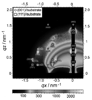
Korgel's team synthesized Si nanocrystals by thermal decomposition of hydrogen silsesquioxane (HSQ), followed by etching with HF, reaction with 1-dodecene, and size-selective precipitation of the obtained nanoparticles. The quantum dots were then dispersed in chloroform and finally drop cast. Two known techniques—called transmission electron microscopy (TEM) and grazing-incidence small-angle X-ray scattering (GISAXS)—were applied to study the ordering of the nanocrystals. "Because the order in these arrangements can influence the properties of the nanomaterials, silicon quantum dot superlattices provide a new playground for understanding and manipulating the properties of silicon in new and unique ways", Korgel says.
More information: Korgel, B., Silicon Nanocrystal Superlattices, ChemPhysChem. dx.doi.org/10.1002/cphc.201200738
Journal information: ChemPhysChem
Provided by Angewandte Chemie


