Breaking the performance barrier of 22-nm CMOS technology

A major initiative has been launched in Europe with a top-ranked project called DUALLOGIC, Dual channel CMOS for (sub)-22 nm high performance logic.
Co-funded by the European Commission’s 7th Framework Program (FP7) in Information and Communication Technologies, DUALLOGIC is the flagship of CMOS R&D in FP7. Mobilizing key European semiconductor IC and equipment manufacturers, top technology development laboratories, research centers and universities, the DUALLOGIC project is an endeavor to shape future CMOS generations beyond today’s 22-nm technology by achieving breakthroughs in nano-electronic materials, equipment, processing and device integration on silicon.
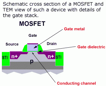
The end of 2007 marked the birth of what Gordon Moore described as the “biggest change in transistor technology in 40 years,” namely the 45-nm CMOS generation. Now in production, this technology features a transistor gate with a metal/high-k dielectric combination instead of polySi/SiO2, which was long considered irreplaceable.
If the heart of the transistor—the gate dielectric—can be changed, any other part of the transistor can be changed eventually as well. The active channel may be the next component to be replaced in an effort to surpass the performance of the 22-nm node.
Charge carriers of germanium feature higher mobility, so replacing silicon in the channel with germanium could enhance transistor performance significantly. Unfortunately, after five years of intensive research, it has now been established that Ge is suitable only for pMOS. Therefore a complementary MOS technology made entirely of Ge is not yet feasible today. Conversely, other semiconductors such as III-V compounds (e.g. GaAs, InGaAs) are indeed suitable for nMOS, but appear to be unsuitable for pMOS. Contrary to what was believed only a few years ago, semiconductors composed of Ge and III-V compounds are not competitors; rather, these materials could complement each other on the same chip.
Based on these findings, the DUALLOGIC project will attempt to cointegrate Ge pMOS and III-V nMOS side-by-side on a complexly engineered substrate on silicon to demonstrate for the first time a dual-channel CMOS technology.
A European consortium of 9 members has been awarded an EC grant of 5.8 M€ for this project. All the necessary resources and expertise have been gathered for the 36-month collaboration to tackle such a challenging goal.
The main objective of the project is to demonstrate that a high-mobility, dual-channel, front-end-of-line (FEOL) CMOS technology is scalable and manufacturable. To achieve this, researchers will employ a Si-compatible process in a 65-nm/200-mm pilot line. Researchers expect that, by the end of 2009, the DUALLOGIC project will determine whether this approach is a viable option for CMOS beyond 22 nm. The results could stimulate further development into a wider sub-22-nm technology platform by integrating dual-channel FEOL with backend and device-architecture modules. Such results could provide a solid basis for a future, even more comprehensive R&D initiative in Europe.
Scientists at the Zurich Research Lab are leading the effort to investigate the optimal materials and material combinations for the transistor gate stacks. Their contributions will involve depositing a suitable high-k gate oxide, defining the best material composition for the metal gate, and depositing active channels using III-V semiconductors.
IBM researchers will investigate both the deposition of III-V for surface channel devices as well as the growth of heterostructures, in which the III-V channel is buried beneath other layers. “It is an enormous challenge to incorporate these new materials efficiently into existing device structures and manufacturing processes,” states Dr. Chiara Marchiori, researcher at IBM’s Zurich Lab. “As members of the DUALLOGIC project, we will endeavor to meet this challenge collaboratively.”
Source: IBM


