This article has been reviewed according to Science X's editorial process and policies. Editors have highlighted the following attributes while ensuring the content's credibility:
fact-checked
proofread
Metasurfaces: Tiny tech with big potential

Imagine manipulating light with ultra-thin, flat sheets instead of bulky lenses and mirrors. That's the promise of metasurfaces, a nanostructure technology that can twist and bend light in ways never before possible.
Metasurfaces are artificially engineered surfaces composed of meticulously designed nanostructures, each smaller than the wavelength of light. By controlling the geometry and arrangement of these tiny structures, scientists can create metasurfaces that precisely control the amplitude, phase, and polarization of light waves at the two-dimensional interface.
This unprecedented control over light's properties unlocks a vast array of potential applications previously unattainable with conventional optics.
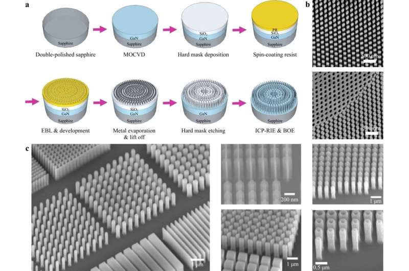
In a new review article published in Light: Advanced Manufacturing, researchers from China discuss the nanofabrication techniques compatible with the manufacture of meta-devices, including maskless and masked lithography. They explore limitations of current fabrication methods and offer solutions to overcome these challenges for advanced nanophotonic applications.
Traditional optical components, such as lenses and prisms, use bulky structures and precise curvatures to manipulate light. On the other hand, metasurfaces achieve similar optical feats within a fraction of the size and complexity. They offer a flat, ultra-thin, lightweight alternative, paving the way for more compact and integrated devices.
The potential applications of metasurfaces span a wide range of fields, including beam steering and focusing, holography and 3D imaging, polarization control and analysis, exotic light beam generation, biomedical imaging and sensing, and optical cloaking.
While metasurfaces offer immense potential, challenges remain in their fabrication and integration. Manufacturing them at large scales with high precision and low cost is a hurdle yet to be overcome. Additionally, fully realizing their miniaturization potential requires addressing the reliance on bulky components in current metasurface devices.
Researchers worldwide are actively addressing these challenges, exploring innovative nanofabrication techniques and integration strategies. The future of metasurfaces promises a world where light is harnessed and manipulated with unprecedented control, leading to transformative advancements in optics, communications, sensing, imaging, and beyond.
More information: Borui Leng et al, Meta-device: advanced manufacturing, Light: Advanced Manufacturing (2024). DOI: 10.37188/lam.2024.005
Provided by TranSpread


