This article has been reviewed according to Science X's editorial process and policies. Editors have highlighted the following attributes while ensuring the content's credibility:
fact-checked
peer-reviewed publication
trusted source
proofread
Scientists pioneer technique to visualize anti-ferroelectric materials

Scientists with the University of Chicago have made significant strides in imaging antiferroelectric materials, a class of materials with unique electrical properties that could open up potential applications in energy storage, sensors, and memory devices.
It is crucial to understand the electronic properties of materials to advance cutting-edge technologies. However, researchers have faced challenges in imaging certain kinds of materials and in turn, discovering their true properties and potential.
"We demonstrated a new method for emerging antiferroelectric materials on the nanoscale," said Sarah King, Asst. Prof. of Chemistry and senior author on the study. "I believe that having new imaging techniques with such high spatial resolution is incredibly powerful. It's going to play a critical role in the development of new materials."
The study was published on June 14th in Science Advances.
Taking a better picture
King's lab uses electron microscopy to study materials to find out how they work and then customize them for various uses. In this case, her team examined materials that have a special ability known as antiferroelectricity.
Antiferroelectric materials are extremely valuable because of their special arrangement of electric dipoles—arrangements of partial positive and negative charges—which perfectly cancel each other out, resulting in no net positive or negative polarization in the material.
Usually there are different ways the electric dipoles can order themselves, and they form what are known as "domains" with different alignments depending on how the material's atoms are arranged.
Crucially, applying an electric field to an antiferroelectric material allows you to switch it to a higher energy state where the electric dipoles don't cancel each other out. This switching behavior makes them particularly fascinating to scientists and engineers looking to unlock their potential, especially for electronics and energy storage.
However, developing these materials has presented challenges, especially when it comes to imaging and characterizing them for modification. Traditional imaging techniques often lack the necessary resolution and contrast to effectively study these materials and their dynamics.
"One of the major hurdles is that we don't have a great way of determining whether something is antiferroelectric because we lack the means to visualize the domains," explained King.
Determined to see their goals clearly, her lab has now pioneered a fresh approach that enables researchers to finally see their domains.

Finding the map
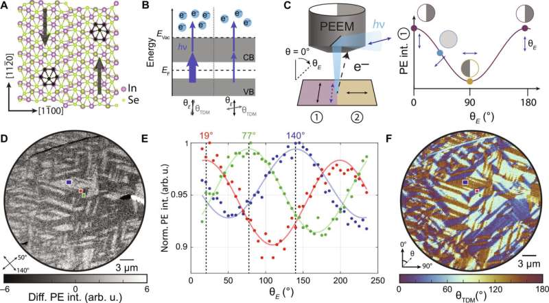
Building on an advanced microscopy technique called polarization-dependent photoemission electron microscopy, the group was able to image in detail the electronic properties and arrangement of domains in a commonly used antiferroelectric material known as indium selenide.
This new method combines polarized light from lasers with electron imaging and offers a more complete picture of a material's properties—mapping the nanoscale arrangement and orientation of the antiferroelectric domains.
Thanks to this breakthrough in imaging technology, King envisions a future in materials science where scientists can thoroughly explore various aspects like domain switching in antiferroelectric and ferroelectric materials and phase transitions.
She's particularly interested in how different properties within materials interact to create ordered states, emphasizing the role order and hierarchy play in domain formation.
The first author on the paper is graduate student Joseph Spellberg; additional authors were undergraduate student Lina Kodaimati, postdoctoral researcher Prakriti Joshi, and graduate student Nasim Mirzajani, as well as Liangbo Liang with Oak Ridge National Laboratory.
More information: Joseph L. Spellberg et al, Electronic structure orientation as a map of in-plane antiferroelectricity in β′-In 2 Se 3, Science Advances (2024). DOI: 10.1126/sciadv.ado2136
Journal information: Science Advances
Provided by University of Chicago


