This article has been reviewed according to Science X's editorial process and policies. Editors have highlighted the following attributes while ensuring the content's credibility:
fact-checked
trusted source
proofread
How semiconductor defects could boost quantum technology

In diamonds (and other semiconducting materials), defects are a quantum sensor's best friend. That's because defects, essentially a jostled arrangement of atoms, sometimes contain electrons with an angular momentum, or spin, that can store and process information. This "spin degree of freedom" can be harnessed for a range of purposes, such as sensing magnetic fields or making a quantum network.
Researchers led by Greg Fuchs, Ph.D. '07, professor of applied and engineering physics at Cornell Engineering, went searching for such a spin in the popular semiconductor gallium nitride and found it, surprisingly, in two distinct species of defect, one of which can be manipulated for future quantum applications.
The group's paper, "Room Temperature Optically Detected Magnetic Resonance of Single Spins in GaN," was published in Nature Materials. The lead author is doctoral student Jialun Luo.
Defects are what give gems their color, and for this reason, they are also known as color centers. Pink diamonds, for example, get their hue from defects called nitrogen-vacancy centers. However, there are many color centers that have yet to be identified, even in materials that are commonly used.
"Gallium nitride, unlike diamond, is a mature semiconductor. It has been developed for wide bandgap high-frequency electronics, and that's been a very intense effort over many, many years," Fuchs said. "You can go and buy a wafer of it; it's in your computer charger, probably, or electric car. But in terms of a material for quantum defects, it has not been explored very much."
In order to search for the spin degree of freedom in gallium nitride, Fuchs and Luo teamed up with Farhan Rana, the Joseph P. Ripley Professor of Engineering, and doctoral student Yifei Geng, with whom they had previously explored the material.
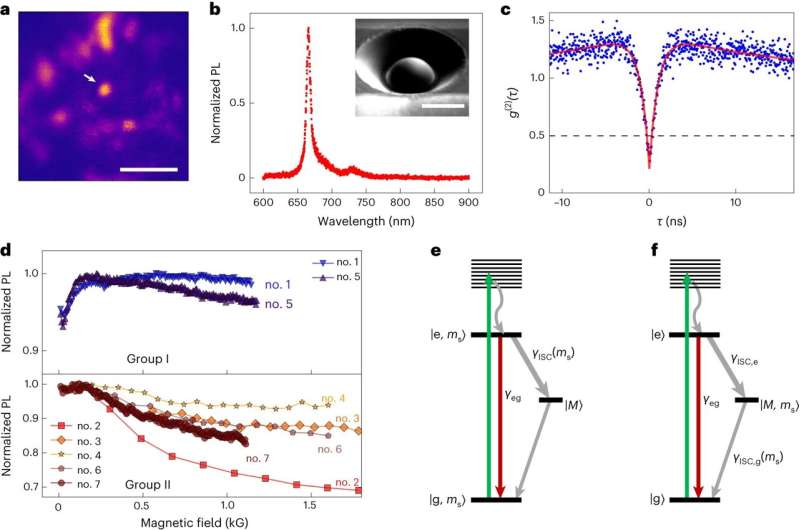
The group used confocal microscopy to identify the defects via fluorescent probes and then conducted a host of experiments, such as measuring how a defect's fluorescence rate changes as a function of the magnetic field and using a small magnetic field to drive the defect's spin resonant transmissions, all at room temperature.
"At the beginning, the preliminary data showed signs of interesting spin structures, but we couldn't drive the spin resonance," Luo said. "It turns out that we needed to know the defect symmetry axes and apply a magnetic field along the correct direction to probe the resonances; the results brought us more questions waiting to be worked out."
The experiments showed the material had two types of defects with distinct spin spectra. In one, the spin was coupled to a metastable excited state; in the other, it was coupled to the ground state.
In the latter case, the researchers were able to see fluorescence changes of up to 30% when they drove the spin transition—a large change in contrast and relatively rare for a quantum spin at room temperature.
"Usually, the fluorescence and spin are tied together very weakly, so when you change the spin projection, the fluorescence might change by 0.1% or something very, very tiny," Fuchs said. "From a technology standpoint, that isn't great because you want a big change so that you can measure it quickly and efficiently."
The researchers then performed a quantum control experiment. They found they could manipulate the ground-state spin and that it had quantum coherence—a quality that allows quantum bits, or qubits, to retain their information.
"That's something that is pretty exciting about this observation," Fuchs said. "There's still a lot of fundamental work to do, and there are many more questions than there are answers. But the basic discovery of spin in this color center, the fact that it has a strong spin contrast of up to 30%, that it exists in a mature semiconductor material—that opens up all kinds of interesting possibilities that we are now excited to explore."
More information: Jialun Luo et al, Room temperature optically detected magnetic resonance of single spins in GaN, Nature Materials (2024). DOI: 10.1038/s41563-024-01803-5
Provided by Cornell University


