This article has been reviewed according to Science X's editorial process and policies. Editors have highlighted the following attributes while ensuring the content's credibility:
fact-checked
peer-reviewed publication
trusted source
proofread
New ways to make ordered wafer-scale chiral carbon nanotube architectures

Chiral materials interact with light in very precise ways that are useful for building better displays, sensors and more powerful devices. However, engineering properties such as chirality reliably at scale is still a significant challenge in nanotechnology.
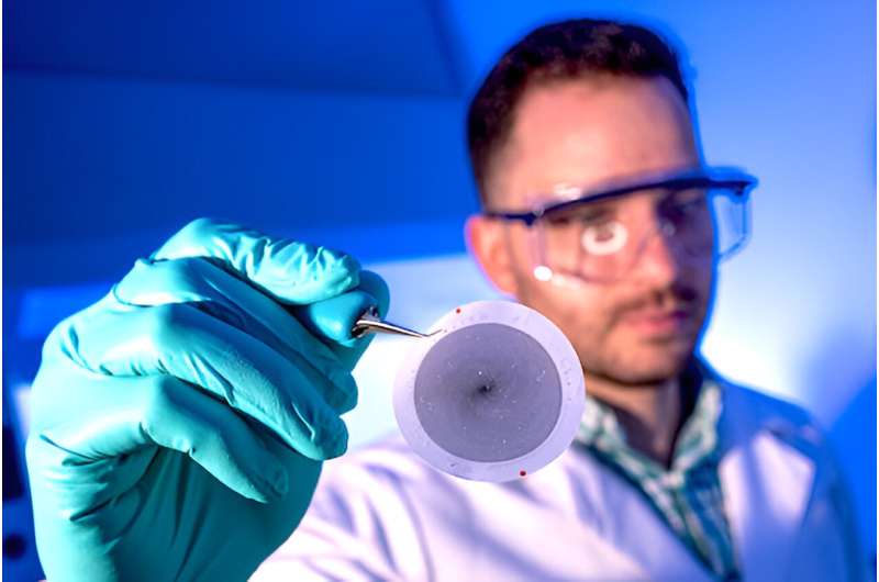
Rice University scientists in the lab of Junichiro Kono have developed two ways of making wafer-scale synthetic chiral carbon nanotube (CNT) assemblies starting from achiral mixtures. According to a study published in Nature Communications, the resulting "tornado" and "twisted-and-stacked" thin films can control ellipticity—a property of polarized light—to a level and in a range of the spectrum that was previously largely beyond reach.
"These approaches have granted us the ability to deliberately and consistently introduce chirality to materials that, until now, did not exhibit this property on a macroscopic scale," said Jacques Doumani, a graduate student in applied physics at Rice and the lead author of the study. "Our methods yield thin, flexible films with tunable chiral properties."
CNTs—hollow cylindrical structures made from carbon atoms—possess remarkable electrical, mechanical, thermal and optical properties. A single-wall CNT has a diameter approximately 100,000 times smaller than that of a single human hair.
The problem is that most ways to make CNTs in greater quantities, which is necessary for use in numerous applications, typically yield heterogeneous, disorderly nanotube assemblies. Such random architectures decrease a material's overall performance.
The ability to create large enough quantities of films in which the nanotubes have the same diameter and orientation could fuel innovation across a broad range of domains, from information systems to medical or energy applications.
"In prior research, we showed that our vacuum filtration technique can achieve nearly perfect alignment of carbon nanotubes at significant scales," said Kono, the Karl F. Hasselmann Professor in Engineering, professor of electrical and computer engineering and materials science and nanoengineering and one of the principal investigators of the paper. "This research allows us to take that work in an exciting new direction by introducing chirality."
The discovery that motion could impart a chiral twist on an orderly CNT arrangement happened entirely by chance.
"It was, quite literally, an unexpected twist," Doumani said, recounting how a shaky pump placed on the same table as the vacuum filtration system caused unintended vibrations which wound the layer of aligned CNTs into a tornadolike spiral.
"These vibrations had a profound impact on the architecture of the assembled carbon nanotubes, prompting us to explore and refine this newfound phenomenon further," he said. "This chance discovery allowed us to recognize that we can design carbon nanotube architectures with desired characteristics by adjusting rotation angles and shaking conditions."
Kono likened the resulting chiral symmetry of the CNT assemblies to a "work of art."
"I am particularly proud of Jacques for pursuing the discovery that we can combine carbon nanotube filtration and shaking to tune the characteristics of these wafer-scale films," Kono said.
The second method of achieving chirality involved stacking highly aligned CNT films at an angle by controlling the number of layers and twisting angles.
"We achieved a remarkable milestone in the deep ultraviolet range, where we set a new record for ellipticity," Doumani said. "What's more, compared to competitors in this space, our technique is very simple to set up. We don't need a complex system to make these films."
The techniques can be used to engineer materials for new optoelectronic devices, such as LEDs, lasers, solar cells and photodetectors. It's also a setup that can potentially be used to make wafer-scale chiral film using other nanomaterials such as boron nitride nanotubes and tungsten diselenide nanotubes.
"This discovery holds promise for various applications," Doumani said. "In pharmaceuticals and biomedicine, it offers potential in biosensing, deep-sea imaging and identifying useful compounds. In communication, it could enhance missile detection, secure communication channels and bolster anti-interference capabilities. In quantum computing engineering, it paves the way for more deterministic photon-emitter coupling.
"We're excited to extend this technique to other types of nanomaterials as well."
More information: Jacques Doumani et al, Engineering chirality at wafer scale with ordered carbon nanotube architectures, Nature Communications (2023). DOI: 10.1038/s41467-023-43199-x
Journal information: Nature Communications
Provided by Rice University


