This article has been reviewed according to Science X's editorial process and policies. Editors have highlighted the following attributes while ensuring the content's credibility:
fact-checked
peer-reviewed publication
trusted source
proofread
Progress in upscaling Si spin and superconducting-based quantum technologies

The long-term vision for quantum computing is the ability to leverage millions of noise-free qubits to address selected problems that are hard to solve with classical computers. Application fields that may benefit from this technology include materials synthesis, pharmaceutical drug development, and cybersecurity, to name a few.
Various quantum computing platforms with diverse types of qubits are under investigation, and worldwide efforts are ongoing to scale up from hundreds to millions of qubits. Having different levels of maturity, each platform has its own needs for scaling up. Common challenges include well-controlled qubit integration in large-size wafer facilities and the need for electronics to interface with the growing number of qubits.
Superconducting quantum circuits have emerged as arguably the most developed platform. The energy states of superconducting qubits are relatively easy to control, and researchers have been able to couple more than a hundred qubits together. This enables an ever-higher level of entanglement—one of the pillars of quantum computing. Also, superconducting qubits with long coherence times (up to several 100µs) and sufficiently high gate fidelities—two important benchmarks for quantum computation—have been demonstrated in lab environments worldwide.
In 2022, imec researchers achieved a significant milestone towards realizing a 300mm CMOS process for fabricating high-quality superconducting qubits. Showing that high-performing qubit fabrication is compatible with industrial processes addresses the first fundamental barrier to upscaling, i.e., improved variability and yield. Among the remaining challenges is the need to develop scalable instrumentation to interface with the growing number of noise-sensitive superconducting qubits.
In the longer term, much is expected from Si-spin-based qubits. Si spin qubits are more challenging to control than superconducting qubits, but they are significantly smaller (nm size vs. mm size)—giving an advantage for upscaling. Also, the technology is highly compatible with CMOS manufacturing technologies, offering wafer-scale uniformity with advanced back-end-of-line interconnection of the Si quantum dot structures. However, Si-based quantum dot structures fabricated with industrial manufacturing techniques typically exhibit a higher charge noise. Their small physical size also makes the qubit-to-qubit and qubit-to-classical control interconnection more challenging.
This article reports on the challenges these platforms face in their race to upscale and on the progress achieved so far.
A cryo-CMOS multiplexer for superconducting qubit readout and control
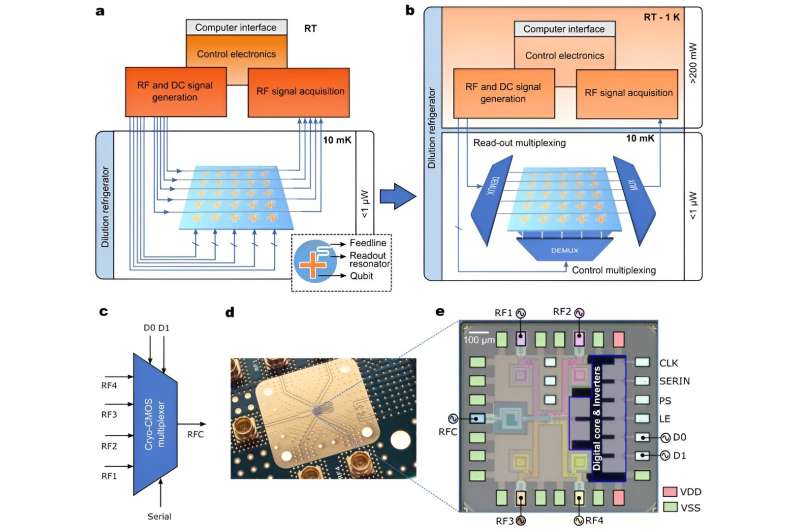
The much-needed increase in qubits requires versatile and scalable solutions to control them and read out meaningful results. In early quantum processors today, external electronics circuits are used with at least one control line per qubit running from the room-temperature stage to the lowest temperature stage of the dilution refrigerator that holds the qubits. This base temperature is as low as 10 milliKelvin (mK) for superconducting quantum computing systems.
Such an approach can be used for up to a few thousand qubits but cannot be sustained for large-scale quantum computers that require dynamic circuit operations such as quantum error correction. Not only do the control and readout lines contribute to a massive I/O bottleneck at the level of the dilution refrigerator, but each wire also brings in heat to the cryogenic system with no budget left to cool them.
An attractive solution is to use CMOS-based cryo-electronics that hold RF (de-) multiplexing elements operating at the base temperature of the dilution refrigerator. Such a solution alleviates the I/O bottleneck as the number of wires that go from room to mK temperatures can be significantly reduced. For the readout, for example, the multiplexers would allow multiple signals from a group of quantum devices to be switched to a common output line at the dilution refrigerator base temperature before leaving the fridge.
This approach has already been demonstrated for Si spin qubit quantum systems. However, thus far, the cryogenics electronics have not been interfaced with superconducting qubits due to their significantly lower tolerance to high-frequency electromagnetic noise. Be it in the form of dissipated heat or electromagnetic radiation, noise can easily disrupt fragile quantum superpositions and lead to errors. That's why the power consumption of the multiplexing circuits should be very low, well below the cooling budget of the dilution refrigerator. In addition, the multiplexers must have good RF performance, in terms of, for example, wideband operation and nanosecond scale switching.
Imec has demonstrated an ultralow power cryo-CMOS multiplexer for the first time that can operate at a record low temperature of 10mK. Being sufficiently low in noise and power dissipation, the multiplexer was successfully interfaced with high-coherence superconducting qubits to perform qubit control with single qubit gate fidelities above 99.9%.
This number quantifies the difference in operation between an ideal gate and the corresponding physical gate in quantum hardware. It is above the threshold for starting experiments like quantum error correction—a prerequisite for realizing practical quantum computers that can provide fault-tolerant results. These results have been published in Nature Electronics.
The multiplexer chip is custom designed at imec and fabricated in a commercial foundry using a 28nm bulk CMOS fabrication technology. Record-low static power consumption of 0.6µW (at a bias voltage, Vdd, of 0.7V) was achieved by eliminating or modifying the most power-hungry parts of a conventional multiplexer circuit as much as possible.
The "easiest" way to run the multiplexer is in static operation mode, which is very useful for performing single qubit characterizations. However, operations involving more than one qubit—such as quantum error correction or large-scale qubit control—will require a different approach allowing concurrent control of multiple qubits within a pulse sequence.
Imec researchers developed an innovative solution involving time division multiplexing of the control signals. This could provide an interesting basis for building future large-scale quantum computing system architectures. Preliminary experiments show that the multiplexer can perform nanosecond-scale fast dynamic switching operations and is hence capable of doing active time division multiplexing while signal crosstalk is sufficiently suppressed.
Currently, the team is working toward implementing a two-qubit gate based on the concept of time division multiplexing.

The experiments described in this work have been set up to contribute to developing large-scale quantum computers by reducing wiring resources. But they also bring innovations to the field of metrology. Throughout the experiments, the ultralow noise performance of the multiplexing circuit at mK temperature was characterized for the first time using imec's superconducting qubits. In other words, the superconducting qubit can be used as a highly sensitive noise sensor, able to measure the performance of electronics that operate at ultralow temperatures and noise regimes that have never been explored before.
A modular integration approach for Si spin qubits fabricated on a 300mm CMOS platform
Si spin qubits are defined by semiconductor quantum dot structures that trap a single spin of an electron or hole. For optimal spin qubit control, the qubit environment must display low charge noise, the gate electrodes must be well-defined with small spacings for electrical tunability, and the spin control structure must be optimized for fast driving with lower dephasing.
High-fidelity Si spin qubits have been repeatedly demonstrated in lab environments in the few-qubit regime. Techniques for processing the qubit nanostructures, such as metal lift-off, are carefully chosen to achieve low noise around the qubit environment. But these well-controlled fabrication techniques have a serious downside: they challenge a further upscaling towards larger numbers of qubits, as they cannot offer the required large-scale uniformity—the very reason these methods were abandoned decades ago in the semiconductor industry at large.
Industrial manufacturing techniques like subtractive etch and lithography-based patterning, on the other hand, can offer wafer-scale uniformity, paving the way to technology upscaling. But they have been observed to degrade the qubit environment easily. Additionally, qubit devices, like the closely spaced gate electrode and the spin control structures, aren't regular transistor structures either and therefore deviate from the typical transistor roadmaps, requiring (costly) new development.
To make the device optimization more complex, the qubit performance depends largely on all these structures and on comprehensive optimizations of the full gate stack, metal electrode design, and spin control modules that are necessary for qubit performance. Nevertheless, the overall device structure should still be compatible with the fabrication methods used for advanced, scaled transistors in commercial foundries to ensure a fair chance at upscaling.
At imec, researchers are tackling this conundrum through careful optimization and engineering of the fab qubit in a modular approach: different qubit elements are separately addressed and optimized as part of a state-of-the-art 300mm integration flow, ensuring forward compatibility with scaling requirements while satisfying the need for dedicated, non-standard device optimization as required by the challenging quantum environment.
Preliminary results on optimized structures look promising, highlighting 300mm fab integration as a compelling material platform for enabling high-quality Si-based spin qubits and upscaling studies. The developments take advantage of the unrivaled uniformity offered by CMOS manufacturing techniques.
More information: Acharya et al, Multiplexed superconducting qubit control at millikelvin temperatures with a low-power cryo-CMOS multiplexer, Nature Electronics (2023). DOI: 10.1038/s41928-023-01033-8
Journal information: Nature Electronics
Provided by IMEC


