This article has been reviewed according to Science X's editorial process and policies. Editors have highlighted the following attributes while ensuring the content's credibility:
fact-checked
trusted source
proofread
Highlighting an 'innovative approach' to research into 2D materials

New research from Lancaster University presents an "innovative approach" to investigating the heat conductivity of novel two-dimensional materials. The work paves the way for creating efficient waste heat scavengers that generate cheap electricity, new compact fridges, and advanced optical and microwave sensors and cameras.
The research, led by Professor of Nanoscience Oleg Kolosov and Ph.D. student Sergio Gonzalez-Munoz, directly measures the heat conductivity of two-dimensional materials (2DMs). It is published in Advanced Materials Interfaces.
Two–dimensional materials are composed of stacks of nearly-perfect tightly bound atomic sheets connected by the weaker van der Waals forces. The typical examples are recently discovered graphene, molybdenum disulfide and the vast range of transition metal dichalcogenides. These are known for their record-breaking electronic and mechanical properties as well as their unique ability to manipulate heat conductance.
In particular, the heat conductivity of 2DMs is key to developing novel highly efficient thermoelectrics, but it is practically impossible to measure thermal conductivity in the nanoscale thin layers of 2DMs.
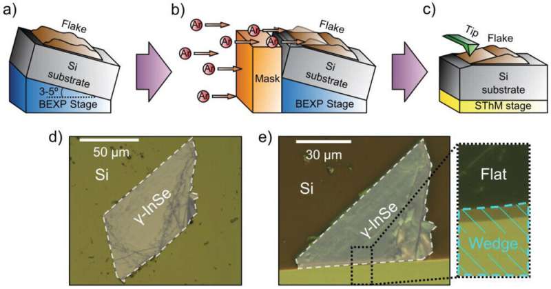
The researchers resolved this challenge by developing a novel scanning thermal microscopy approach allowing them to directly measure the heat conductivity for both the in-plane and cross-plane directions of two-dimensional materials. Both planes are very different due to the atomic structure of the material.
Professor Kolosov said, "This work explains the origin of the record-breaking thermoelectric performance of multi-layered structures of two-dimensional materials which we researchers described in an earlier paper. We enable such measurements and demonstrated this with the example of the potentially highly performing 2DM thermoelectric indium selenide (InSe)."
He said the research had implications for future technological development.
More information: Sergio Gonzalez‐Munoz et al, Direct Measurements of Anisotropic Thermal Transport in γ‐InSe Nanolayers via Cross‐Sectional Scanning Thermal Microscopy (Adv. Mater. Interfaces 17/2023), Advanced Materials Interfaces (2023). DOI: 10.1002/admi.202370056
Provided by Lancaster University


