This article has been reviewed according to Science X's editorial process and policies. Editors have highlighted the following attributes while ensuring the content's credibility:
fact-checked
peer-reviewed publication
proofread
Researchers explore the potential of a novel compound for X-ray detection and imaging

Prof. Pan Xu's team at the Institute of Solid State Physics, Hefei Institutes of Physical Science (HFIPS), Chinese Academy of Science (CAS), in collaboration with Zheng Xiaojia at the Chinese Academy of Engineering Physics (CAEP), and other researchers, discovered the remarkable potential of one-dimensional (1D) δ-phase formamidinium lead iodide (δ-FAPbI3) as an advanced material for X-ray detection.
The related results were published in ACS Nano.
Perovskite materials with excellent optoelectronic properties have great potential for direct X-ray detection, with multiple orders of magnitude higher sensitivity and lower detection limits than current commercial detector materials, and are expected to dramatically reduce the radiation dose rate in radiographic imaging.
However, the preparation of polycrystalline wafers generates a large number of grain boundaries and pores, which leads to severe ion migration and further causes device instability and current drift, severely limiting the imaging resolution of the detectors and future commercial applications.
In this research, researchers focus their attention on the unique characteristics of 1D δ-FAPbI3. This yellow phase compound possessed high ion mobility barriers, low Young's modulus, and exceptional long-term stability.
"We consider it an ideal candidate for high-performance X-ray detection," said Ye Jiajiu, a postdoctoral researcher, "Especially the dense wafer devices prepared by a cold isostatic pressing process can detect X-rays with high sensitivity and low detection limits."
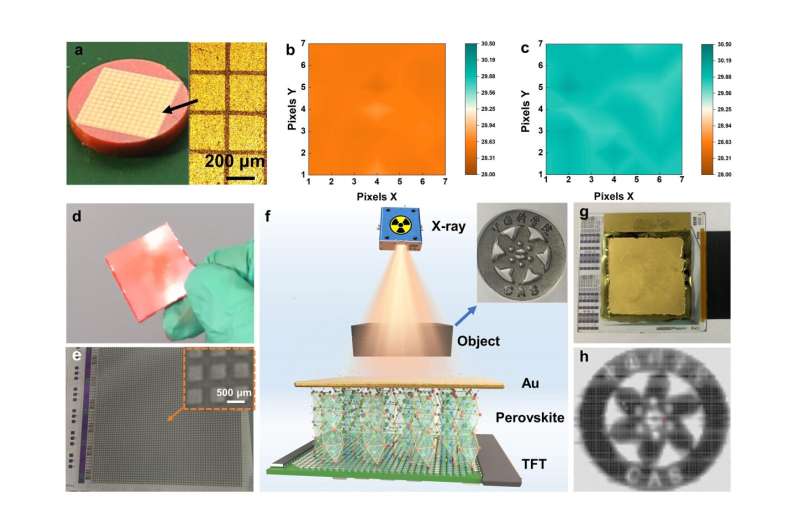
In addition, researchers fabricated an X-ray imager with large-size δ-FAPbI3 wafers integrated on a thin-film transistor (TFT) backplane, realizing two-dimensional multi-pixel X-ray imaging and demonstrating the feasibility of the δ-FAPbI3 wafer detector for ultra-stable imaging applications.
Prof. Pan expressed optimism about the future prospects of this technology. "This study provides a new design idea and material selection system for perovskite application in X-ray imaging," he said.
More information: Zihan Wang et al, Supple Formamidinium-Based Low-Dimension Perovskite Derivative for Sensitive and Ultrastable X-ray Detection, ACS Nano (2023). DOI: 10.1021/acsnano.3c02476
Journal information: ACS Nano
Provided by Hefei Institutes of Physical Science, Chinese Academy of Sciences


