This article has been reviewed according to Science X's editorial process and policies. Editors have highlighted the following attributes while ensuring the content's credibility:
fact-checked
proofread
3D-printed facet-attached microlenses (FaML) could overcome photonic packaging challenges

Photonic integrated circuits (PICs) are on the verge of significant disruption through the unlocking of novel applications. This success largely relies on advanced wafer-level miniaturized photonic device fabrication, combining outstanding functionality and robustness with unprecedented performance and scalability.
However, while cost-efficient mass production of PIC has become widely available through dedicated foundry services, scalable photonic packaging and system assembly still represent a significant challenge and an obstacle towards accelerated commercial uptake.
Specifically, package-level optical chip-to-chip and fiber-to-chip connections often rely on so-called butt coupling, where device facets are brought close or in direct physical contact. This approach usually requires high-precision active alignment with sub-micrometer accuracy, thus complicating assembly processes. Moreover, matching the mode fields can be challenging, particularly when connecting waveguides with vastly different refractive-index contrasts.
In a new paper published in Light: Advanced Manufacturing, a team of scientists led by Dr. Yilin Xu and Professor Christian Koos from Karlsruhe Institute of Technology (KIT) have demonstrated that 3D-printed facet-attached microlenses (FaML) can overcome the scalability challenges of PIC-based solutions.

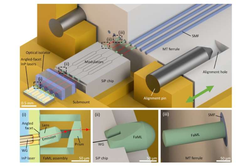
FaML can be printed with high precision to the facets of optical components using multi-photon lithography, thereby offering the possibility to shape the emitted beams by freely designed refractive or reflective surfaces. Specifically, the beams can be collimated to a comparatively large diameter independent of the device-specific mode fields. This approach relaxes axial and lateral alignment tolerances.
Their findings mean that costly active alignment becomes obsolete and can be replaced by passive assembly techniques based on machine vision or simple mechanical stops. Moreover, the FaML concept allows inserting discrete optical elements, such as optical isolators or polarization beam splitters, into the free-space beam paths between PIC facets.
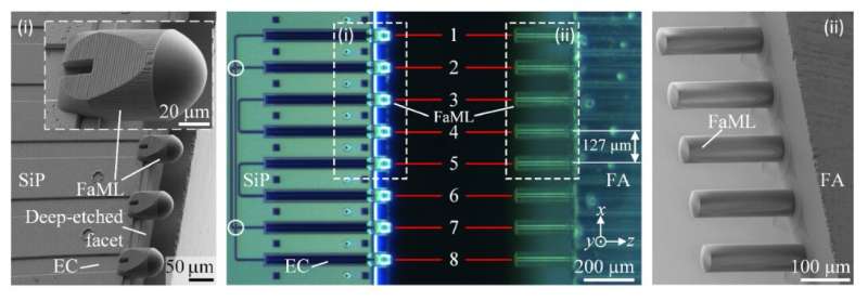
Building upon their previous work, the researchers showed the scheme's viability and versatility in a series of selected demonstrations of high technical relevance. In the first set of experiments, they coupled fiber arrays to arrays of edge-coupled silicon photonic (SiP) chips, reaching insertion losses of 1.4 dB per interface with a translational lateral 1 dB alignment tolerance of ± 6 μm.
This is the lowest loss demonstrated for an edge-emitting SiP waveguide interface with micron-scale alignment tolerances. The researchers further demonstrated that their scheme's outstanding alignment tolerance allows contactless pluggable fiber-chip interfaces using conventional injection-molded parts.

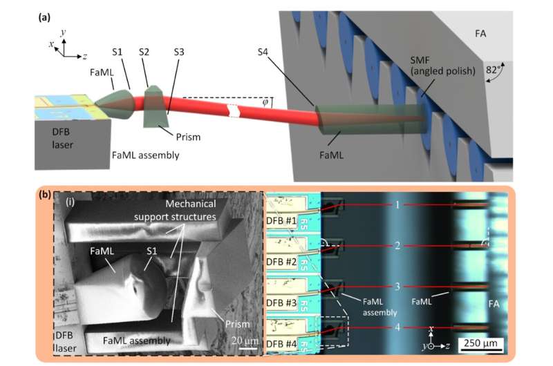
In a second set of experiments, the researchers demonstrated free-space transmission over distances in the mm range, using standard machine-vision techniques for alignment. A third set of experiments is finally dedicated to interfaces between InP lasers and SMF arrays. In these experiments, the researchers demonstrated the coupling of planar devices through non-planar beam paths comprising only tilted optical surfaces, thus offering ultra-low back-reflection.
Based on their exemplary demonstrations of the outstanding versatility of the FaML approach, the researchers believe that their concept opens an attractive path towards advanced photonic system assembly that may overcome most of the current challenges. Opening a path towards scalable and flexible photonic packaging concepts that complement wafer-level mass fabrication of the underlying PIC, the FaML concept addresses one of the most stringent challenges of integrated optics today.
More information: Yilin Xu et al, 3D-printed facet-attached microlenses for advanced photonic system assembly, Light: Advanced Manufacturing (2023). DOI: 10.37188/lam.2023.003
Provided by TranSpread


