This article has been reviewed according to Science X's editorial process and policies. Editors have highlighted the following attributes while ensuring the content's credibility:
fact-checked
peer-reviewed publication
trusted source
proofread
Spectroscopic micro-ellipsometer unveils atomic-level thickness measurements of 2D materials

Two-dimensional (2D) material flakes consist of single to few atomic layers, granting them extraordinary quantum properties, which are not observed in everyday materials. As a result, these materials hold immense potential for both industrial applications and advanced research.
Traditionally, ellipsometry has been a widely adopted optical technique for noninvasive measurement of thin-film thicknesses. However, commercial ellipsometers face limitations when it comes to measuring areas smaller than 50-60 microns, while 2D flakes often have lateral dimensions of only a few microns.
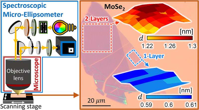
Addressing this significant challenge, Prof. Ronen Rapaport and Ralfy Kenaz of Hebrew University have developed and patented a system and method for a microscope-integrated ellipsometer, namely, Spectroscopic Micro-Ellipsometer (SME).
This cutting-edge instrument allows for fast and atomic-level precise measurements of thin-film thicknesses in extremely small areas, down to a mere 2 microns wide within a few seconds. The instrument's exceptional performance has already been validated in a separate publication, solidifying its credibility and reliability.
In a recent publication in the journal ACS Nano, Hebrew University's researchers utilized this innovative micro-ellipsometer to tackle the modern scientific conundrum of measuring and mapping the thicknesses of atomically thin 2D material flakes. The findings unequivocally demonstrate the micro-ellipsometer's ability to successfully measure and map the thicknesses of diverse 2D material flakes, enabling the determination of their number of atomic layers.
The implications of this research extend to a multitude of industries and research fields that deal with microstructures and paves the way for highly accurate optical investigations of microstructures, opening doors to advancements in technology and scientific exploration. By introducing the application of the well-established and highly sensitive ellipsometry technique to microstructures, this research presents a novel and invaluable system for researchers and industries alike.
The Spectroscopic Micro-Ellipsometer can be commissioned in thin film industry for quality control of wafers, for characterizing 2D devices and nanoscale metamaterials and investigating crystal structure of nanoparticles among many other potential applications.
More information: Ralfy Kenaz et al, Thickness Mapping and Layer Number Identification of Exfoliated van der Waals Materials by Fourier Imaging Micro-Ellipsometry, ACS Nano (2023). DOI: 10.1021/acsnano.2c12773
Journal information: ACS Nano
Provided by Hebrew University of Jerusalem


