This article has been reviewed according to Science X's editorial process and policies. Editors have highlighted the following attributes while ensuring the content's credibility:
fact-checked
peer-reviewed publication
trusted source
proofread
Molding two-dimensional organic molecule crystals

Recently, a group of illegal counterfeiters was apprehended for producing around 400 fake luxury jewelry items using molds. They were able to create hundreds of faked luxury items simply after pouring molten metal into molds produced from the original jewelry. Similarly, in the molecular world, a template scaffold can produce an endless amount of molecular crystals of any shape or form.
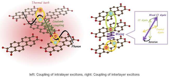
Professor Sunmin Ryu of and Ph.D. candidate Dogyeong Kim (Department of Chemistry) from Pohang University of Science and Technology (POSTECH), and their team of researchers have succeeded in growing layered structures of two-dimensional molecular crystals (perylenetetracarboxylic dianhydride or PTCDA) and confirmed their intralayer and interlayer excitonic interactions (coupling). The findings from the study were recently published in Nature Communications.
2D organic molecular solids are sought after as the next-generation semiconductor materials for applications such as flexible display. Understanding the properties of excitons in crystals is crucial for future usage of 2D organic molecules in various applications. However, past research on the excitons has hit a roadblock due to organic molecules' tendency to aggregate into formless clumps without a specific structure.
The team at POSTECH created a layered structure by stacking up 2D organic molecular crystals using hexagonal boron nitride (hBN) as a mold. Boron nitride is an insulating material that does not conduct electricity. The team utilized it as a scaffold to successfully produce 2D organic molecular crystals and stacked these crystal layers on top of each other.
The researchers first determined the two-dimensional molecular crystals' structure and arrangement by analyzing their degrees of optical absorption and patterns of electron diffraction. The team also confirmed intralayer and interlayer coupling of the molecular excitons after selectively separating the stacked 2D organic molecular crystals into the desired number of layers (or thicknesses).
In a single layer, the molecular vibrations decreased as the temperature decreased, creating a more stable environment. As a result, excitons within the crystal were able to interact with relatively distant excitons, which was confirmed through changes in fluorescent energy. Moreover, as multiple layers were stacked, there was a continuous variation in the overall orientation of molecular transition dipoles due to the 'mixing' of interlayer excitons with intralayer excitons.
However, once the thickness of the crystal reached a certain threshold, the direction of the interlayer molecular dipoles ceased to change and converged towards a single direction. It was observed that by manipulating the temperature and thickness of the layered structure, control over the interaction between excitons could be achieved.
Professor Sunmin Ryu explained, "Through this study, we have demonstrated the ability to control the physical properties of organic-molecule-based 2D materials and the movement of excitons," adding his expectation for "various applications in organic semiconductors and solar power generation."
More information: Dogyeong Kim et al, In-plane and out-of-plane excitonic coupling in 2D molecular crystals, Nature Communications (2023). DOI: 10.1038/s41467-023-38438-0
Journal information: Nature Communications
Provided by Pohang University of Science and Technology


