This article has been reviewed according to Science X's editorial process and policies. Editors have highlighted the following attributes while ensuring the content's credibility:
fact-checked
peer-reviewed publication
proofread
Visualizing spatial distribution of electric properties at microscales with liquid crystal droplets

Microelectromechanical systems (MEMS) involve the use and development of micron-sized electrical devices such as microelectrodes, sensors, and actuators that are integrated into computer and smartphone chips. Fabricating such integrated MEMS devices is usually a challenging task as these devices often deviate from their original design owing to the defects introduced during their fabrication and operation. This, in turn, limits their performance. Therefore, it is crucial to identify and rectify these defects.
One way to identify and rectify these defects is by measuring the spatial distribution of electric properties of these devices. However, standard sensor probes do not offer the required spatial resolution, and can only determine the spatially averaged-out electric properties. Due to this, it is possible to detect only the presence of defects, not their location.
Fortunately, liquid crystal droplets (LCDs)–micron-sized droplets of soft matter with molecular orientational order–offer hope on this front. LCDs respond strongly to external stimuli such as an electric field, and can thus act as a high-resolution probe.
Capitalizing on this promise, Dr. Shinji Bono and Prof. Satoshi Konishi from Ritsumeikan University, Japan, have now utilized LCDs for visualizing the electric properties of microstructured electrodes via a technique called particle imaging electrometry. Their findings were published in Scientific Reports.
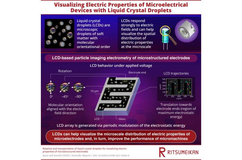
Dr. Bono explains the research methodology. "The LCDs were dispersed on microelectrodes arranged in a comb-like structure atop a glass slab. Their molecular orientations, determined using polarized optical microscopy, were randomly distributed when the electric field was absent. Then, a voltage was applied across the electrodes."
Because of this, the LCDs between the electrodes and in front of the electrode ends underwent rotation, their molecular orientations lining up perpendicular and parallel to the electrodes, respectively. This alignment, revealed by COMSOL simulations performed by the researchers, corresponded to the direction of the electric field, and occurred faster with increasing voltage. The relaxation frequency of rotation was found to vary as the square of the applied voltage.
Further, at high voltages, the LCDs showed translation (linear motion) towards the electrodes, especially their endpoints, the regions with maximum electrostatic energy density. Based on this behavior, the researchers could produce an array of LCDs via periodic modulation of the energy density in a micro-capacitive MEMS device. The LCD array, in turn, served as a periodic modulator of the refractive index, a number characterizing the light bending ability of a material.
These results thus demonstrate that the electric properties of microelectrodes and microelectric devices can be visualized simply by observing the rotational and translational behavior of LCDs under an electric field. Moreover, the technique provides a high spatial resolution (10 μm) as well as high detection accuracy (5 μV/μm).
In light of these features, Prof. Konishi has high hopes for its applications. "It will help improve the design and fabrication of integrated microelectrical devices by providing information on the defect location, which so far has remained unavailable. In turn, more sophisticated MEMS technology may become available soon," he concludes.
More information: Shinji Bono et al, Rotation and transportation of liquid crystal droplets for visualizing electric properties of microstructured electrodes, Scientific Reports (2023). DOI: 10.1038/s41598-023-31026-8
Journal information: Scientific Reports
Provided by Ritsumeikan University


