September 6, 2022 feature
Liquid cell transmission electron microscopy analysis of semiconductor nanocrystals
. DOI: 10.1126/sciadv.abq1700")
Semiconductor nanocrystals of different sizes and shapes can govern the optical and electrical properties of materials. Liquid cell transmission electron microscopy (LCTEM) is an emerging method to observe nanoscale chemical transformations and inform the precise synthesis of nanostructures with expected structural features. Researchers are investigating the reactions of semiconductor nanocrystals with the method to study the highly reactive environment produced via liquid radiolysis during the process.
In a new report now published in Science Advances, Cheng Yan and a research team in Chemistry and Materials Science at the University of California Berkeley, and the Leibniz Institute of Surface Engineering, Germany, harnessed the radiolysis process to replace the single particle etching trajectory of prototypical semiconductor nanomaterials. Lead selenide nanotubes used during the work represented an isotropic structure to retain the cubic shape for etching through a layer-by-layer mechanism. The anisotropic arrow-shaped cadmium selenide nanorods maintained polar facets with cadmium or selenium atoms. The trajectories of transmission liquid cell electron microscopy revealed how the reactivity of specific facets in liquid environments governed the nanoscale shape transformations of semiconductors.
Optimizing liquid cell transmission electron microscopy (LCTEM)
Semiconductor nanocrystals contain widely tunable optical and electrical properties that depend on their size and shape for a diverse array of applications. Materials scientists have characterized the reactivity of specific bulk crystal facets toward growth and etching reactions to develop the most arbitrary patterns in top-down bulk semiconductor processing. The multiple facets of nanocrystals and their reaction mechanism make them interesting for direct investigation. The thermodynamics of colloidal nanocrystals can influence the organic-inorganic interfaces defining them. Liquid cell transmission electron microscopy offers the required space-time resolution to observe nanoscale dynamics, such as the self-assembly process. The team therefore sandwiched an aqueous pocket containing nanocrystals between the ultrathin carbon layers of two transmission electron microscopy grids, and used tris (hydroxymethyl) aminomethane hydrochloride (tris·HCl), an organic molecule to regulate the etching of sensitive semiconductor nanocrystals.
Existing research on LCTEM and nanocrystals are limited to noble metals due to their inability to regulate the chemical environment during radiolysis, causing reactive materials to degrade. Recent research suggests a possibility to design new environments for LCTEM, to observe single-particle etching trajectories of reactive nanocrystals. During the experiments, the tris·HCl additive regulated the electrochemical potential of the etching process, and the team used kinetic modeling to estimate the concentration and electrochemical potential of the amine radical species in the liquid cell.
Proof-of-concept
As proof of concept, the scientists obtained representative transmission electron microscopy images of a lead selenide nanocube in vacuum and gathered a time-series of images during layer-by-layer etching of lead selenide nanocrystals. The outcome of LCTEM imaging showed the formation of a substance with higher image contrast around the lead selenide nanocrystals as a product of etching reactions, it appears that during the etching process, selenium oxidized and dispersed into the liquid to facilitate the formation of lead chloride, with chloride ions in the lead pocket. When compared to the cubic lattice of lead selenide, wurzite cadmium selenide featured an anisotropic lattice with alternating layers of cadmium and selenium atoms. During the growth of wurzite cadmium selenide nanocrystals, the surfactant ligands favorably bound to the cadmium regions to facilitate the fast growth of selenium regions.
Yan et al. presented the structure of cadmium selenide nanorods resolved via high-angle annular dark field scanning transmission electron microscopy in vacuum. The scientists generated the images by collecting electrons scattered to high angles by atoms in the material to develop mass-thickness image contrast, where cadmium was brighter than selenium. The team similarly performed in situ etching experiments on arrow-shaped cadmium selenide nanorods.
-
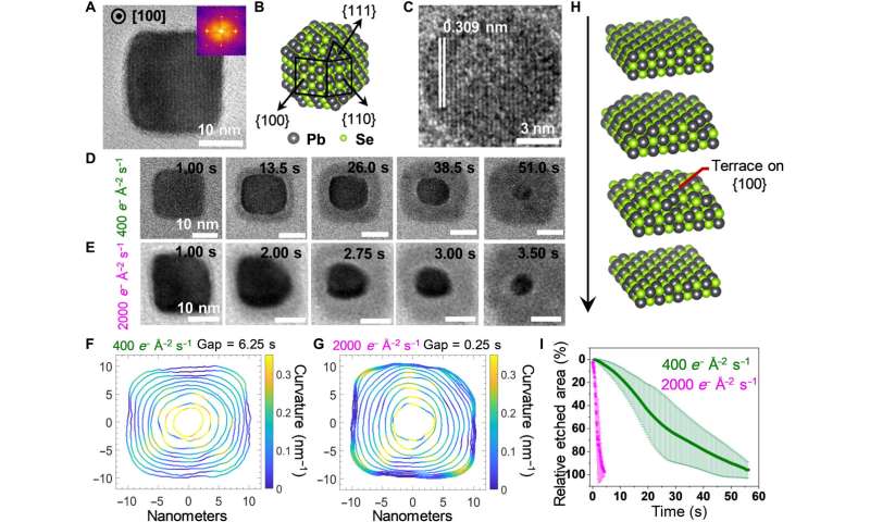
Structural characterization and etching trajectories of PbSe nanocubes. (A) Representative static TEM image of a PbSe nanocube oriented along the [100] zone axis. (B) Atomistic model of a truncated PbSe nanocube exposing different facets. (C) The LCTEM image captured near the end of an etching trajectory, exhibiting the characteristic d-spacing of {200} lattice planes of PbSe. (D and E) Time-lapse LCTEM images recorded at the electron fluence rates of 400 e− Å−2 s−1 (D) and 2000 e− Å−2 s−1 (E), respectively. (F and G) Outlines of the nanocrystals plotted with equal time gaps for illustrating the evolving shapes and local curvatures of PbSe nanocrystals recorded at 400 e− Å−2 s−1 (F) and 2000 e− Å−2 s−1 (G), respectively. (H) Scheme of the layer-by-layer etching mechanism, which proceeds via terrace intermediates. (I) The time-dependent plots of the relative etched area normalized to the projected area of the PbSe nanocube at the starting frame. Credit: Science Advances (2022). DOI: 10.1126/sciadv.abq1700 -
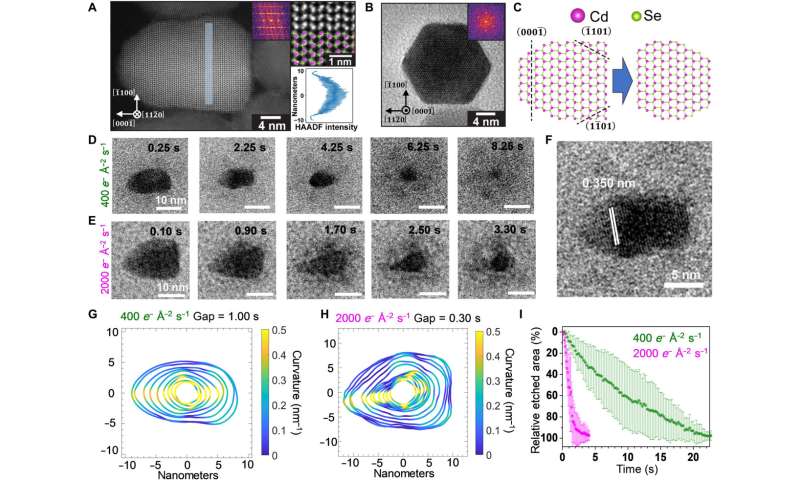
Structural characterization and etching trajectories of CdSe nanorods. (A) AC-HAADF-STEM image of a wurtzite CdSe nanorod projected along the [110] zone axis (left). The enlarged inset (top right) verifies the polarity of the nanorod: The tip of the rod is terminated by Se (green), while the bottom is terminated by Cd (pink). The line profile of HAADF-STEM intensity in the shaded segment (left) projected along the [00] axis is included in the bottom right. (B) TEM image of a nanorod oriented along the c axis showing a hexagonal projection. (C) Lattice models of a CdSe nanorod projected along the [110] axis (left) and the truncated structure (right) formed by selectively etching the Se-terminated facets. (D and E) Time-lapse LCTEM images recorded at electron fluence rates of 400 e− Å−2 s−1 (D) and 2000 e− Å−2 s−1 (E), respectively. (F) The LCTEM image exhibiting the characteristic d-spacing of {0002} lattice planes. (G and H) Outlines of the nanocrystals plotted with equal time gaps for illustrating the evolving shapes and local curvatures of CdSe nanorods at 400 e− Å−2 s−1 (G) and 2000 e− Å−2 s−1 (H), respectively. (I) Time-dependent plots of the relative etched area normalized to the projected area of the CdSe nanorod at the starting frame. Credit: Science Advances (2022). DOI: 10.1126/sciadv.abq1700 -
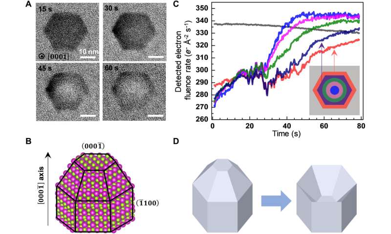
The etching trajectory of a wurtzite CdSe nanocrystal viewed along the [000] axis. (A) Time-lapse LCTEM images recorded at 400 e− Å−2 s−1. (B) Atomistic model of the CdSe nanocrystal with the (000) facet pointing up. (C) Time-dependent plot of the average electron fluence rates detected in different color-coded segments (inset) of the LCTEM images. Gray color corresponds to the background region surrounding the nanocrystal. (D) 3D illustration of the etching process showing that the selective etching of the Se-terminated (000) facet causes the tip to transform into a concave pit in the nanocrystal. Credit: Science Advances (2022). DOI: 10.1126/sciadv.abq1700
Outlook
In this way, Cheng Yan and colleagues used liquid cell electron microscopy (LCTEM) to show the possibility of directly examining the facet-dependent reactivity of colloidal nanocrystals at the nanoscale. The method offered real-time, continuous structural trajectories, in contrast to classical methods. Existing research had already highlighted the effect of the inclusion or removal of ligands on the self-assembly and etching of nanocrystals in LCTEM experiments.
The team showed how sensitive nanomaterials such as lead selenide can be studied using LCTEM and highlighted the inclusion of organic additives such as tris·HCl to regulate the radiolytic redox environment in liquid cell electron microscopy. Future studies can enable the potential to gain real-time information about the transformation of an array of functional nanostructures with increasing complexity using core/shell nanocrystals, as well as those assembled via inorganic-organic interfaces.
More information: Chang Yan et al, Facet-selective etching trajectories of individual semiconductor nanocrystals, Science Advances (2022). DOI: 10.1126/sciadv.abq1700
Yu-Ho Won et al, Highly efficient and stable InP/ZnSe/ZnS quantum dot light-emitting diodes, Nature (2019). DOI: 10.1038/s41586-019-1771-5
Journal information: Science Advances , Nature
© 2022 Science X Network


