February 16, 2022 feature
A robotic method for assembling complex van der Waals solids

2D van der Waals crystals, a class of materials that exhibit strong in-plane covalent bonds and weak interlayer interactions, have recently become the focus of numerous research studies due to their plethora of unique electrical, optical, and mechanical properties. Curiously, when a hybrid vertical stacking of different sheets of van der Waals crystals is assembled, it gains new properties absent from any of its constituent layers.
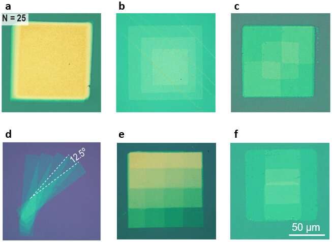
Recently, researchers at University of Chicago, Cornell University, and University of Michigan have been exploring a new robotic technique to assemble intricate van der Waals structures so that their hybrid properties may be more efficiently studied. In a newly published paper in Nature Nanotechnology, the team introduced a robotically-automated method for the 4D assembly van der Waals solids, building on techniques for wafer-scale 2D materials synthesis and clean stacking of materials under vacuum introduced in their previous works.
"While the techniques we developed in the past allowed us to stack 2D materials layers of ~one square centimeter, it was difficult to create structures with micron-resolved, intricate in-plane designs," Andrew Ye, one of the primary authors of the study, told Phys.org. "Ultimately, we wanted a technique that allows us to take advantage of wafer-scale material and the cleanliness of vacuum-stacking in the context of manufacturing structures with micron-scale, geometric sophistication. Our new method allows us to do that."
Currently, many heterostructures comprised of 2D materials are built using exfoliated 2D flakes. However, these flakes can have very random shapes, so the geometry of the resulting, assembled structures can appear somewhat "disarranged."
"Contrarily to these techniques, our newly developed method allows us to manufacture structures with deliberate geometries," Ye explained. "This is because we start out with a wafer of material, then cleanly pattern it into arrays of discrete 'pixel'-ized units. These pixels become the building blocks for the assembled complex structures."
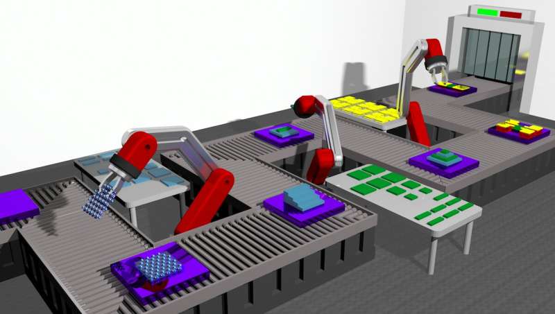
To assemble van der Waals structures, Ye and his colleagues used an instrument they custom built, comprised of a high-vacuum-chamber with (X, Y, Z, and θ) actuators that holds a carefully designed polymer stamp. The vacuum chamber ensures that materials inside it remain pristine during manufacturing processes.

The four-axis actuators allows the instrument to control the movements of the polymer stamp with high levels of precision. Finally, the polymer stamp can be used to methodically pick up material pixels from a chip and gently place them onto another.
"Because our process is highly automated, we can run our machine without operator control and assemble structures at roughly 30 layers per hour," Ye explained. "This is an order of magnitude quicker than what could be done before."
The recent paper introduces a new, valuable paradigm that can be used to manufacture complex van der Waals heterostructures, starting from wafer-scale, synthesized materials. This advantageous new method could help to advance the assembly of heterostructures based on 2D materials, moving beyond existing and small-scale laboratory techniques.
"In the context of academic research, we show that this technique could be used to quickly study permutations of different materials within a single structure (such as for exploring new optical or electrical phenomena) and to study the properties of multilayer θ-twisted single-crystal 2D materials, which is of interest in the condensed-matter-physics community," Ye said.
In the future, the assembly method introduced by this team of researchers could be used to manufacture electronics based on 2D materials on a large scale. While existing laboratory-based techniques can typically only be used to reliably manufacture heterostructures that are a few microns in size, the method proposed by Ye and his colleagues could enable the large-scale manufacturing of 100-micron-sized and complex van der Waals solids.
"We are now planning to further develop the use of electrodes into the robotic stacking process," Ye added. "Furthermore, there are a lot of interesting physics properties in multilayer θ-twisted single-crystal 2D materials that we would like to delve deeper into."
More information: Andrew J. Mannix et al, Robotic four-dimensional pixel assembly of van der Waals solids, Nature Nanotechnology (2022). DOI: 10.1038/s41565-021-01061-5
Journal information: Nature Nanotechnology
© 2022 Science X Network


