Improving the conductivity of metal nanoelectrodes achieved via plasmon-enhanced laser nanosoldering

In a new publication from Opto-Electronic Advances, the research groups of Professor Xuan-Ming Duan from Jinan University Guangzhou, China and Professor Mei-Ling Zheng from the Institute of Physics and Chemistry of Chinese Academy of Sciences, Beijing, China discuss plasmon-enhanced nanosoldering of silver nanoparticles for high-conductive nanowires electrodes.
In recent years, metal nanowire electrodes have been widely used in new photodetectors, flexible circuits, solar cells, touch panels, etc. Femtosecond laser direct writing (FsLDW), based on multi-photon absorption induced photoreduction, is used to build Ag nanowires (NWs) for engineered patterns in two and three dimensions with submicron resolution. This technology has unique advantages of high resolution, true three-dimensionality, and flexibility. However, the Ag NWs constructed by FsLDW are composed of the small Ag nanoparticles (NPs). There are voids or polymer coatings between Ag NPs, resulting in poor electrical conductivity. Therefore, in order to increase the conductivity of the direct-write Ag NWs and reduce its resistance, it is necessary to reduce the gap between the Ag NPs and increase the contact area to reduce the energy dissipation of the conductive electrons in the electrode. For the Ag NWs electrodes by laser irradiation, the photothermal effect can significantly increase the contact area of adjacent Ag NPs and improve the conductivity of the Ag NWs electrode. This protocol provides a novel and high-efficiency solution for achieving large-area, high-uniformity, and patterned nanowire conductivity enhancement.
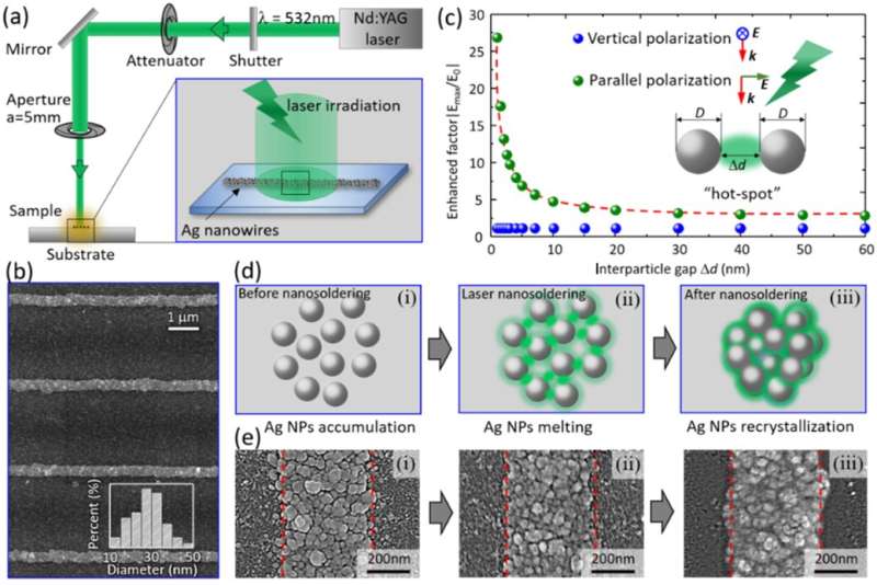
The research group of Professor Xuan-Ming Duan from the Institute of Photonics Technology of Jinan University and the research group of Professor Mei-Ling Zheng from the Institute of Physics and Chemistry, Chinese Academy of Sciences jointly proposed an optical method for enhancing the electric conductivity of the Ag NWs by plasmon-enhanced laser nanosoldering (PLNS) (Figure 1a). This method cleverly uses the structural characteristics of Ag NWs fabricated by FsLDW. The NWs are composed of aggregates of NPs reduced by the multiphoton absorption effect, and plasmons "hot-spots" are generated among the NPs under laser irradiation (Figure 1b, c). The local Ag NPs connection or soldering at room temperature achieved by plasmon-enhanced photothermal effect, which can significantly increase the contact area between Ag NPs and improve the conductivity of NWs. Unlike the traditional heating annealing, the heating part of this method is only localized near the hot spot, which will not cause thermal damage to the substrate (Figure 1d, e).
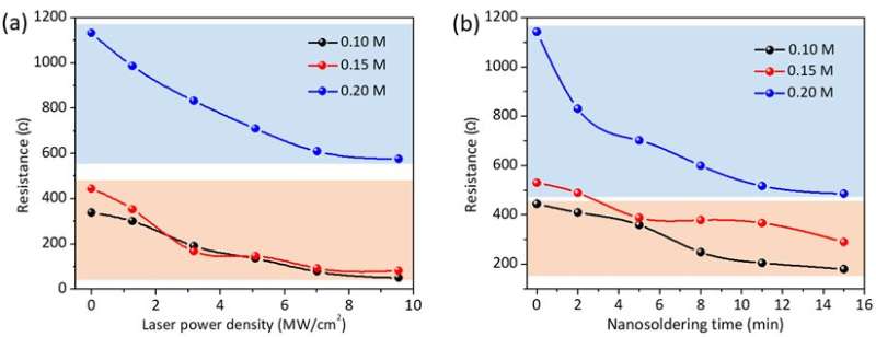
This laser nanosoldering technology does not require complicated post-processing, and directly increases the conductivity of the Ag NWs electrode fabricated by FsLDW. Further study of the influence of laser power density and nanosoldering time on the conductivity of Ag NWs show that the resistance of Ag NWs decreases significantly with the increase of laser power density or nanosoldering time. As shown in Figure 2a, b, the increasing of conductivity tends to be saturated. This is because the NPs and nanogaps available for nanosoldering gradually decrease as the laser irradiation time increases. Under the optimized experimental conditions, the laser power density was 9.55 MW/cm2 and the nanosoldering time was 15 minutes. The maximum conductivity was increased to 2.45×10⁷ S/m, which was 39 percent of bulk Ag. This research provides an efficient, controllable and low-cost method to improve the conductivity of Ag NWs, and promotes the application of FsLDW of Ag NWs electrodes as active SERS substrates, transparent electrodes, capacitors, light-emitting diodes, and thin-film solar cells.

More information: Yuan-Yuan Zhao et al, Plasmon-enhanced nanosoldering of silver nanoparticles for high-conductive nanowires electrodes, Opto-Electronic Advances (2021). DOI: 10.29026/oea.2021.200101
Provided by Compuscript Ltd


