MXene-GaN van der Waals metal-semiconductor junctions for high performance photodetection

High levels of dark current and noise have ailed metal-semiconductor-metal (MSM) photodetectors for years. Recently, scientists in China demonstrated that by replacing conventional metals with MXene, the dark current and noise of MSM multiple quantum well photodetectors can be significantly improved.
The proliferation of the Internet of Things (IoT) has sparked intense interest of photodetectors (PD) as they are widely used in sensing, detection, data transport and processing. The coming 5G-enabled IoT (5G-IoT) will require new performance criteria such as massive connectivity, ultra-low latency and ultra-reliability for huge number of IoT devices. To meet these demands, metal-semiconductor-metal (MSM) photodetectors have received much attention for their high response speed, simple fabrication process and feasibility of integration with field effect transistor (FET) technology.
However, the conventional fabrication process will induce chemical disorder and defect states at the metal-semiconductor interfaces, leading to significant dark current and noise. Additionally, opaque metals are usually placed on top of the active light absorption region, which will reflect part of the incident light and thus reduce the responsivity of MSM photodetectors.
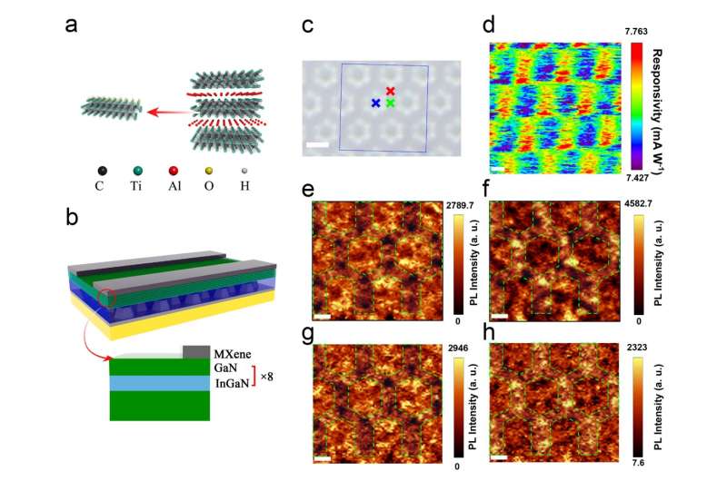
In a new paper published in Light Science & Application, a team of scientists led by Professor Jiang Wu from Institute of Fundamental and Frontier Sciences, University of Electronic Science and Technology of China has demonstrated a high performance MXene-GaN-MXene based multiple quantum well photodetector prepared on patterned sapphire substrate by facile drop casting.
MXene, a new type of two-dimensional (2D) materials discovered in 2011, has many charming properties, such as metallic conductivity, mechanical flexibility, hydrophilia, good transmittance and chemical stability, which enable MXene to be processed in solution at low temperatures and under ambient conditions. Additionally, the widely tunable work function makes MXene a great candidate for ohmic or Schottky contacts with various semiconductor materials. More importantly, 2D materials consist of in-plane covalently bonded atomic layers that interact weakly with each other in the out-of-plane direction. When deposited on bulk semiconductor materials, MXene-semiconductor van der Waals junctions formed at the interface are free of chemical disorder and have less defect states, which could avoid the Fermi level pinning effect and reduce the reverse tunneling currents.
The multiple quantum well photodetector proposed by Jiang et al was grown on the patterned sapphire substrate, which can promote the epitaxial lateral overgrowth (ELOG) mode and consequently reduce the defect density in GaN epilayers and the MXene was employed to replace the conventional metals, Au/Cr. The MXene-GaN-MXene based multiple quantum well photodetector showed significantly improved responsivity, dark current and noise in the blue-green light spectrum range compared with the conventional counterpart, making it a potential candidate for under water optical detection and communication. The improvements were attributed to the low-defect MXene-GaN van der Waals interfaces. More interestingly, thanks to the high quality MXene-GaN van der Waals junctions, which can suppress the dark current and noise hence distinguish minor spatial variation of the photocurrent in the order of nanoamps, the localized light focusing and enhancement by the patterned sapphire substrate were observed.
More information: Lingzhi Luo et al, MXene-GaN van der Waals metal-semiconductor junctions for high performance multiple quantum well photodetectors, Light: Science & Applications (2021). DOI: 10.1038/s41377-021-00619-1
Journal information: Light: Science & Applications
Provided by Chinese Academy of Sciences


