Scientists devise method for gentle laser processing of perovskites at nanoscale

Scientists of Far Eastern Federal University (FEFU) in partnership with colleagues from ITMO University, and universities in Germany, Japan, and Australia, have developed a method for precise, fast and high-quality laser processing of halide perovskites (CH3NH3PbI3), promising light-emitting materials for solar energy, optical electronics, and metamaterials. Structured by very short laser pulses at the femtosecond scale, perovskites turned out to be functional nanoelements marked by unprecedented quality. A related article is published in Small.
Perovskites were discovered in the first half of the 19th century in the Ural (Russia) in the form of a mineral consisting of calcium, titanium and oxygen atoms. Today, due to unique properties, perovskites are up-and-coming materials for solar energy and the development of light-emitting devices for photonics, i.e. LEDs and microlasers. They hit the top of the most scrutinizing materials that attract the interest of scientific groups from all around the world.
The major drawback is complicated processing. Perovskites easily degrade under the influence of an electron beam, liquids or temperature, losing the properties scientists are so interested in. This significantly complicates the manufacturing of functional perovskite nanostructures by means of common methods as electron beam lithography.
Scientists from FEFU (Vladivostok, Russia) and ITMO University (St. Petersburg, Russia) teamed up with foreign colleagues and solved this problem by proposing a unique technology for the processing of organo-inorganic perovskites using femtosecond laser pulses. The output was high-quality nanostructures with controlled characteristics.
"It is very difficult to nanostructurize conventional semiconductors, such as gallium arsenide, using a powerful pulsed laser," says Sergey Makarov, a leading researcher at ITMO University's Faculty of Physics and Engineering, "The heat is scattered in all directions and all the thin, sharp edges are simply distorted by this heat. It's like if you try to make a miniature tattoo with fine details, but due to the paint spreading out under the skin, you will just get an ugly blue spot. Perovskite has poor thermal conductivity, so our patterns turned out very precise and very small."
Laser scribing of perovskite films into individual blocks is an important technological step of the modern solar cell production chain. So far the process was not very accurate and being rather destructive for the perovskite material as its outermost sections lost functional properties due to temperature degradation. The new technology can help to solve this problem allowing fabrication of high-performing solar cells.
"Perovskite represents a complex material consisting of organic and inorganic parts. We used ultrashort laser pulses for fast heating and targeted evaporation of the organic part of perovskite that proceeds at rather low temperature of 160 C0. Laser intensity was adjusted in such a way to produce melting/evaporation of the organic part leaving inorganic one unaffected. Such nondestructive processing allowed us to achieve an unprecedented quality of produced perovskite functional structures," said Alexey Zhizhchenko, a researcher at the FEFU School of Engineering.
Scientists of FEFU and ITMO University pointed to three areas where their development can give tangible results.
The first is the recording of information that the user can read only under certain conditions. "We have demonstrated the relevance of our approach by producing diffraction gratings and microstrip lasers with the ultimately small width of only 400 nanometers. Such characteristic dimensions pave the way towards development of active elements of future optical communication chips and computers," said Alexey Zhizhchenko.
Secondly, with the help of a laser, one can change the visible color of a perovskite fragment with no dye applied. Material may come like yellow, black, blue, red, depending on the needs.
"This may be utilized to perform solar panels of all colors of the rainbow. The modern architecture allows covering the entire surface of the building by solar panels, the point is not all customers want plain black panels," Sergey Makarov said.
The third application is the manufacturing of nanolasers for optical sensors and optical chips that transmit information via photons rather than electrons.
-
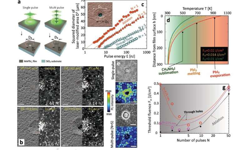
Figure 1. Single- and multi-pulse laser ablation of MAPbI3 films. a) Schematic illustration of single- and multi-pulse laser processing of glass-supported MAPbI3 films with focused Gaussian-shaped fs pulses. b) Side-view (view angle of 30°) SEM images of 425-nm thick MAPbI3 film irradiated by a single fs pulse at increased pulse energy E ranging from 2.44 to 25.2 nJ. For better understanding, each SEM image was obtained by combining signals from two SEM detectors: InLens detector signal (right part of each image) and mixed SE/InLens signal. Diameter of the ablation area is marked by orange circle in each image. Scale bar corresponds to 500 nm. c) Squared diameter D2 of the ablation area (solid orange markers) and the through hole (hollow markers) produced in the 425-nm thick MAPbI3 film under single- (N = 1) and multi-pulse (N = 5) irradiation versus applied pulse energy E (plotted in logarithmic scale). For multi-pulse irradiation, the total incident pulse energy is considered. d) In-depth peak temperature profiles of laser-irradiated MAPbI3 calculated at variable incident peak fluences F. e) Correlated SEM and confocal PL images of μm-sized through holes drilled in the 425-nm thick MAPbI3 film by single-pulse and multi-pulse (N = 5) irradiation. Scale bars indicate 2 μm. g) Threshold incident fluence Fth required for MAPbI3 film ablation (orange markers) and hole formation (hollow markers) versus the number of applied laser pulses N measured for variable film thickness h. Solid curves provide the data based on theoretical assessments. Dotted curve fits the statistically averaged experimental data for ablation threshold. Each pulse in the train has identical energy, while the total incident pulse energy is considered for fluence calculations. Credit: FEFU press office -
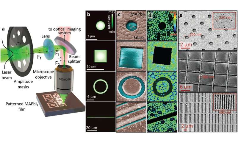
Laser projection lithography used for advanced fs-laser patterning of perovskite films. a) Scheme of experimental setup used for fs-laser projection lithography. b) Focal-plane intensity profiles of various flat-top laser beams used for direct patterning of perovskite films. c) Representative false-color side-view (view angle of 30°) SEM images of isolated openings produced in MAPbI3 film using generated flat-top intensity profiles. d) Corresponding confocal PL maps in the vicinity of laser-patterned areas. e) Series of SEM images of 425-nm thick MAPbI3 film patterned with circular-shaped microholes, square-shaped openings, and 400-nm width through nanoslits. Credit: FEFU press office -
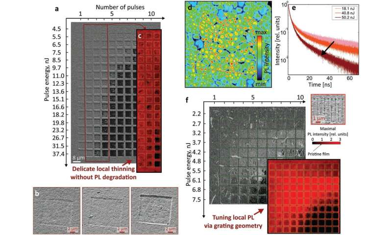
Tailoring local PL properties via precise laser-induced thinning and nanopatterning of MAPbI3 films. a) Large-scale top-view SEM image showing 425-nm thick MAPbI3 film irradiated with square-shape flat-top laser beam at gradually varying fluence F (vertical axis) and number of applied pulses N (horizontal axis). b) Representative side-view SEM images of several ablated area produced at fixed number of pulses and increased pulse energy. c) Wide-field PL image of the laser-patterned area marked with red rectangle. d) High-resolution confocal PL image of the laser-modified area of MAPbI2 film. The laser-irradiated area is marked by dashed lines. e) TR-PL decays for square-shaped MAPbI3 film areas patterned at different fluences. f) Correlated SEM and wide-field PL images of the MAPbI3 film patterned with 800-nm period surface gratings of different depths produced by varying the applied fluence F and number of applied pulses N. Inset SEM image showing close-up view on the single pixel containing imprinted surface gratings Credit: FEFU press office -
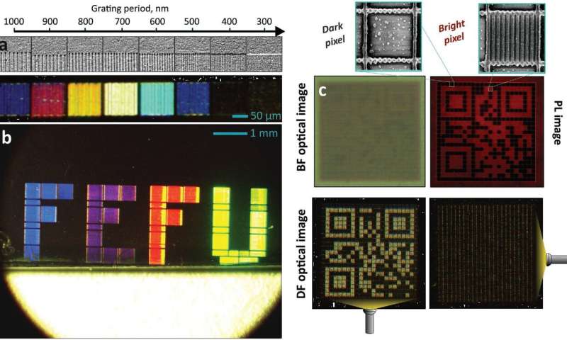
Laser patterning of MAPbI3 for optical encryption and surface coloring. a) Close-up SEM images of the laser-imprinted surface gratings of variable period ranging from 300 to 1000 nm (left panel) as well as dark-field optical image of the 100 × 100 μm2 surface gratings tuned by period within similar range and visualized with 0.15-NA dry microscope objective (right panel). b) DF optical image of mm-scale “FEFU” letters inscribed onto the surface of 425-nm thick MAPbI3 film by recording surface gratings with variable periods. The color of each letter is tuned by the grating period. c) Bright-field optical and PL images of laser-encrypted QR code (top panel). Two inset SEM images show morphology of two (“bright” and “dark”) types of pixels used for QR code encryption. The side of individual pixel is 7.5 × 7.5 μm2. Dark-field optical images of similar laser-encrypted QR code observed upon illumination from different sides indicated by orange arrow (bottom panel). Credit: FEFU press office -
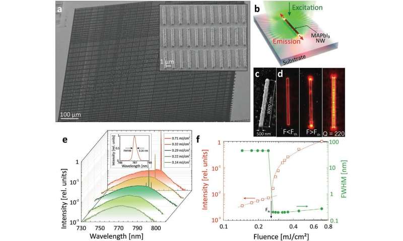
Lasing performance of the imprinted MAPbI3 nanowires (NWs). a) Large-scale SEM image of an array of laser-imprinted MAPbI3 NWs of variable length L and width w. Inset provides magnified SEM image showing reprodusibility of the fabrication process and NW’s facets. b) Schematic of the photoexcitation/emission of the isolated MAPbI3 NW. c) Close-up side-view (view angle of 40°) SEM image of representative isolated NW with w = 500 nm and L = 8000 nm. d) PL image of the same NW pumped at below- (F < Fth) and above-threshold fluences (F > Fth). Right-most image shows the calculated near-field intensity distribution of the Fabry–Perot mode supported by the NW. e) PL spectra of the MAPbI3 NW at different pump fluences. f) Intensity (red markers) and full-width at half-maximum (green markers) at the emission wavelength (λlas ≈ 787 nm) as a function of pump fluence. Credit: FEFU
Simple, fast and cost-effective production of such elements could bring about a new era of computer technology working on the principles of controlled light. Processing of perovskites according to the proposed technology gives a chance to get thousands, even hundreds of thousands of nanolasers per minute. The introduction of the technology to industry will draw the world closer to the development of optical computers.
"Another key feature of the proposed technology is that it allows layer-by-layer thinning of the perovskites. This opens the way to design and fabricate more complicated 3-D microstructures from perovskite, for example, micro-scale vortex-emitting lasers, which are highly demanded for information multiplexing in next-generation optical communications. Importantly, such processing preserves and even improves the light-emitting properties of thinned layer passivated due to modification of chemical composition," said team member Aleksandr Kuchmizhak, research fellow at the FEFU Center for Neurotechnology, VR and AR.
More information: Alexey Y. Zhizhchenko et al, Light‐Emitting Nanophotonic Designs Enabled by Ultrafast Laser Processing of Halide Perovskites, Small (2020). DOI: 10.1002/smll.202000410
Journal information: Small
Provided by ITMO University


