Invention opens the door to safer and less expensive X-ray imaging

Medical imaging, such as X-ray or computerised tomography (CT), may soon be cheaper and safer, thanks to a recent discovery made by chemists from the National University of Singapore (NUS).
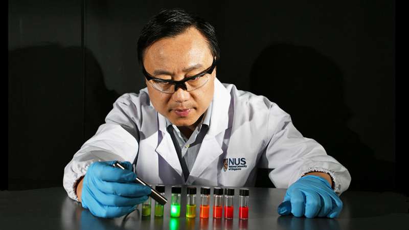
Professor Liu Xiaogang and his team from the Department of Chemistry under the NUS Faculty of Science had developed novel lead halide perovskite nanocrystals that are highly sensitive to X-ray irradiation. By incorporating these nanocrystals into flat-panel X-ray imagers, the team developed a new type of detector that could sense X-rays at a radiation dose about 400 times lower than the standard dose used in current medical diagnostics. These nanocrystals are also cheaper than the inorganic crystals used in conventional X-ray imaging machines.
"Our technology uses a much lower radiation dose to deliver higher resolution images, and it can also be used for rapid, real-time X-ray imaging. It shows great promise in revolutionising imaging technology for the medical and electronics industries. For patients, this means lower cost of X-ray imaging and less radiation risk," said Prof Liu.
The team's research breakthrough was the result of a collaborative effort with researchers from Australia, China, Hong Kong, Italy, Saudi Arabia, Singapore and the United States. It was first published in the online edition of Nature on 27 August 2018, and a patent for this novel technology has been filed.
Nanocrystals light the way for better imaging
X-ray imaging technology has been widely used for many applications since the 1890s. Among its many uses are medical diagnostics, homeland security, national defence, advanced manufacturing, nuclear technology, and environmental monitoring.
A crucial part of X-ray imaging technology is scintillation, which is the conversion of high-energy X-ray photons to visible luminescence. Most scintillator materials used in conventional imaging devices comprise expensive and large inorganic crystals that have low light emission conversion efficiency. Hence, they will need a high dose of X-rays for effective imaging. Conventional scintillators are also usually produced using a solid-growth method at a high temperature, making it difficult to fabricate thin, large and uniform scintillator films.
To overcome the limitations of current scintillator materials, Prof Liu and his team developed novel lead halide perovskite nanocrystals as an alternative scintillator material. From their experiments, the team found that their nanocrystals can detect small doses of X-ray photons and convert them into visible light. They can also be tuned to light up, or scintillate, in different colours in response to the X-rays they absorb. With these properties, these nanocrystals could achieve higher resolution X-ray imaging with lower radiation exposure.
To test the application of the lead halide perovskite nanocrystals in X-ray imaging technology, the team replaced the scintillators of commercial flat-panel X-ray imagers with their nanocrystals.
"Our experiments showed that using this approach, X-ray images can be directly recorded using low-cost, widely available digital cameras, or even using cameras of mobile phones. This was not achievable using conventional bulky scintillators. In addition, we have also demonstrated that the nanocrystal scintillators can be used to examine the internal structures of electronic circuit boards. This offers a cheaper and highly sensitive alternative to current technology," explained Dr. Chen Qiushui, a Research Fellow with the NUS Department of Chemistry and the first author of the study.
Using nanocrystals as scintillator materials could also lower the cost of X-ray imaging as these nanocrystals can be produced using simpler, less expensive processes and at a relatively low temperature.
Prof Liu elaborated, "Our creation of perovskite nanocrystal scintillators has significant implications for many fields of research and opens the door to new applications. We hope that this new class of high performance X-ray scintillator can better meet tomorrow's increasingly diversified needs."
Next steps and commercialisation opportunities
To validate the performance of their invention, the NUS scientists will be testing their abilities of the nanocrystals for longer times, and at different temperatures and humidity levels. The team is also looking to collaborate with industry partners to commercialise their novel imaging technique.
More information: Qiushui Chen et al. All-inorganic perovskite nanocrystal scintillators, Nature (2018). DOI: 10.1038/s41586-018-0451-1
Journal information: Nature
Provided by National University of Singapore


