AI implications: Engineer's model lays groundwork for machine-learning device

In what could be a small step for science potentially leading to a breakthrough, an engineer at Washington University in St. Louis has taken steps toward using nanocrystal networks for artificial intelligence applications.
Elijah Thimsen, assistant professor of energy, environmental & chemical engineering in the School of Engineering & Applied Science, and his collaborators have developed a model in which to test existing theories about how electrons move through nanomaterials. This model may lay the foundation for using nanomaterials in a machine learning device.
"When one builds devices out of nanomaterials, they don't always behave like they would for a bulk material," Thimsen said. "One of the things that changes dramatically is the way in which these electrons move through material, called the electron transport mechanism, but it's not well understood how that happens."
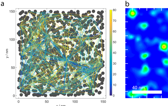
Thimsen and his team based the model on an unusual theory that every nanoparticle in a network is a node that is connected to every other node, not only its immediate neighbors. Equally unusual is that the current flowing through the nodes doesn't necessarily occupy the spaces between the nodes—it needs only to pass through the nodes themselves. This behavior, which is predicted by the model, produces experimentally observable current hotspots at the nanoscale, the researcher said.
In addition, the team looked at another model called a neural network, based on the human brain and nervous system. Scientists have been working to build new computer chips to emulate these networks, but these chips are far short of the human brain, which contains up to 100 billion nodes and 10,000 connections per node.
"If we have a huge number of nodes—much larger than anything that exists—and a huge number of connections, how do we train it?" Thimsen asks. "We want to get this large network to perform something useful, such as a pattern-recognition task."
Based on those network theories, Thimsen has proposed an initial project to design a simple chip, give it particular inputs and study the outputs.
"If we treat it as a neural network, we want to see if the output from the device will depend on the input," Thimsen said. "Once we can prove that, we'll take the next step and propose a new device that allows us to train this system to perform a simple pattern-recognition task."
The results of their work were published in advanced online publication of The Journal of Physical Chemistry C.
More information: Qinyi Chen et al, Visualizing Current Flow at the Mesoscale in Disordered Assemblies of Touching Semiconductor Nanocrystals, The Journal of Physical Chemistry C (2017). DOI: 10.1021/acs.jpcc.7b04949
Journal information: Journal of Physical Chemistry C
Provided by Washington University in St. Louis


