June 26, 2017 weblog
A functional prototype nonvolatile ferroelectric domain wall memory

(Phys.org)—A team of researchers from institutions in Australia, the U.S. and China has developed a functional prototype nonvolatile ferroelectric domain wall memory. In their paper published on the open access site Science Advances, the group describes their prototype, its properties and how well it worked.
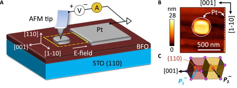
A ferroelectric domain wall is a topological structure with defects that separate regions of uniform polarization—as the researchers note, the discovery of conductivity in such structures has led to a new field of science called "domain wall nanoelectronics." The science essentially covers the wall as a means of storing information—a binary state can be read or written in such memory devices by inducing or removing a conductive wall. They can also be read non-destructively, just as with conventional memory technology. In this new effort, the researchers created a prototype using nanofabricated electrodes that they designed for use specifically with their wall memory, which, they note, was scalable to below 100nm.
Ferroelectric materials are similar to ferromagnetic materials in that they have a permanent dipole moment. The obvious difference is the former moment is electrical while the latter is magnetic, which means that ferroelectric materials can be oriented by exposure to an electric versus a magnetic field. Like ferromagnetics, they have domain walls—but they are much smaller, allowing for the creation of much smaller memory materials, typically in the 1nm range. This makes them smaller by a factor of 10 than current silicon CMOS structures. Creating a memory device involved building a structure in which it was possible to create and destroy walls using electrical pulses. They built their memory structures by using nanolithography to create Pt/Ti patterns on thin film BiFeO3 which could be used as electrodes.
The researchers report that wall materials such as theirs are able to store data on multiple levels because of their unique resistance states, which allows for tuning. They also note that a device using such memory requires less energy to store information than conventional memory. Memory for their prototype could be read at voltages less than 3 V and the team claims it also has a reasonably high OFF-ON ratio of approximately 103 and that it is robust.
More information: Nonvolatile ferroelectric domain wall memory, Science Advances 23 Jun 2017: Vol. 3, no. 6, e1700512, DOI: 10.1126/sciadv.1700512
Abstract
Ferroelectric domain walls are atomically sharp topological defects that separate regions of uniform polarization. The discovery of electrical conductivity in specific types of walls gave rise to "domain wall nanoelectronics," a technology in which the wall (rather than the domain) stores information. This paradigm shift critically hinges on precise nanoengineering of reconfigurable domain walls. Using specially designed nanofabricated electrodes and scanning probe techniques, we demonstrate a prototype nonvolatile ferroelectric domain wall memory, scalable to below 100 nm, whose binary state is defined by the existence or absence of conductive walls. The device can be read out nondestructively at moderate voltages (<3 V), exhibits relatively high OFF-ON ratios (~103) with excellent endurance and retention characteristics, and has multilevel data storage capacity. Our work thus constitutes an important step toward integrated nanoscale ferroelectric domain wall memory devices.
Journal information: Science Advances
© 2017 Phys.org


