Collaboration enhances optical chip design process

A unique collaboration between a U.S. telecommunications equipment provider and a Department of Energy (DOE) Office of Science national laboratory has helped dramatically improve design cycle times for future high-speed optical networking components.
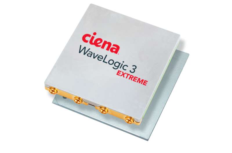
Computer scientists and mathematicians from Lawrence Berkeley National Laboratory's (Berkeley Lab) Computing Sciences organization worked with engineers at Ciena, a leading networking company, to speed up the process by which Ciena validates the design of its ASIC (application-specific integrated circuit) chips. The collaboration grew out of the existing relationship between Ciena, a pioneer in high-bandwidth optical transport technology, and the DOE's Energy Sciences Network (ESnet), which uses Ciena products to support its high-speed network.
"Modern science requires fast global networks like ESnet, and almost all DOE network traffic happens to run over optical gear from Ciena," said Inder Monga, director of ESnet. "ESnet doesn't transport quite as much traffic as, say, Google, but we have the unique challenge of coping with massive single data streams from detectors and instruments like the Large Hadron Collider, the world's largest and most powerful particle accelerator. This means we need to exploit leading-edge networking components, and we're often early adopters of those components."
To help Ciena better utilize computational methods in designing and producing their next-generation optical networking products, John Shalf and James Sethian of Berkeley Lab's Computational Research Division (CRD) demonstrated the feasibility of accelerating computational verification of Forward Error Correction (FEC) codes, which are commonly used in optical transmission equipment for controlling errors in data transmission.
Simulating 9 Quadrillion Bits of Data
To do this they modified a random number generator library called MRG8 (multiple recursive generator with 8th-order recursion), which was developed by Kenichi Miura, a Berkeley Lab affiliate. Ciena's ASIC designers, led by Kim Roberts, then used 8 million supercomputing hours at Berkeley Lab's National Energy Research Scientific Computing Center (NERSC)—provided by NERSC Director Sudip Dosanjh through the Director's Discretionary Reserve—to test and validate the efficacy of the enhanced FEC codes in the Ciena modems. The parameter study made use of a Task Farmer developed by NERSC's Shane Canon to support high-throughput parameter research such as the Ciena FEC code study.
To show the benefits of this technology, the team simulated sending 9 quadrillion bits of data in a noisy environment, where the channel impairments caused about 500 trillion of these bits to be received in error, explained Masoud Ebrahimi, an engineer at Ciena.
"Our FEC mechanism corrected all the 500 trillion errors and ensured us that the bit error rate is below 10-16," Ebrahimi said.
"Without custom ASICs to perform the calculations required for high-speed FEC processing, modern high-speed networking would just not be possible," Roberts said. "FEC is a way of adding extra information to an information signal, so that in case anything is lost or corrupted during transmission, the original data stream can be recovered, up to a point."
The process of validating FEC algorithms requires running a set of sample experiments millions of times, to track when and where any transmission errors occur, explained Sethian, who leads Berkeley Lab's Mathematics Group and the Center for Advanced Mathematics for Energy Research Applications. To improve this process and the FEC code itself, the Berkeley Lab team had to figure out how to seed the experiments to ensure that they were truly random and not secretly correlated or duplicated.
Using the parallel processing resources at NERSC had a dramatic impact on the time it took to run the experiments and validate the design of the FEC algorithm. With NERSC resources, Ciena was able to dramatically expand the scope of their study on a compressed timescale.
"We thought we could take advantage of massively parallel processing to run these things in parallel rather than sequentially," Sethian said. "And in the process we found that there turns out to be more efficient and optimal ways to call these random seeds and random generators to take advantage of these architectures."
Truly Random Numbers
To scale up on the parallel machine—in this case, NERSC's Edison system—required ensuring that the random numbers were truly random and that each of the processors was sampling a completely different space in terms of the random number generator, Shalf added.
"A conventional random number generator follows a predictable "pseudo-random" sequence that repeats itself eventually," he explained. "If you're not careful, you can find yourself repeating the same sequence and not explore as large of a space as you had originally expected. Dr. Miura's MRG8 generates a much longer pseudo-random number sequence before it repeats itself, and also enables each of the parallel processors to be assigned its own starting point in the sequence that is guaranteed to not overlap. MRG8 provides stronger guarantees that a larger space of FEC codes can be explored using parallel computation."
Ciena has now completed the various runs, evaluated the results, and now planning on next-steps. Monga sees this project as the beginning of an ongoing collaboration that could yield additional design and process improvements.
"If the entire industry is pushed forward just a little bit by this collaboration, the market will move forward, new technologies will evolve. That's good for DOE science," Monga said. "We look forward to this partnership continuing to benefit the networking community."
Provided by Lawrence Berkeley National Laboratory


