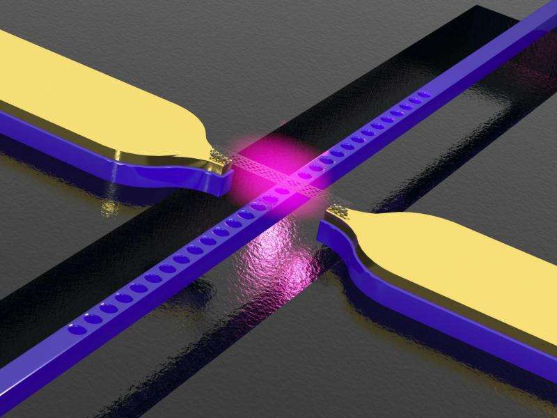
Waveguide with integrated carbon nanotubes for conversion of electric signals into light

Worldwide growing data volumes make conventional electronic processing reach its limits. Future information technology is therefore expected to use light as a medium for quick data transmission also within computer chips. Researchers under the direction of KIT have now demonstrated that carbon nanotubes are suited for use as on-chip light source for tomorrow's information technology, when nanostructured waveguides are applied to obtain the desired light properties. The scientists now present their results in Nature Photonics.
On the large scale, data transmission by light has long become a matter of routine: Glass fiber cables as light waveguides transmit telephone and internet signals, for instance. For using the advantages of light, i.e. speed and energy efficiency, also on the small scale of computer chips, researchers of KIT have made an important step from fundamental research towards application. By the integration of smallest carbon nanotubes into a nanostructured waveguide, they have developed a compact miniaturized switching element that converts electric signals into clearly defined optical signals.
"The nanostructures act like a photonic crystal and allow for customizing the properties of light from the carbon nanotube," Felix Pyatkov and Valentin Fütterling, the first authors of the study of KIT's Institute of Nanotechnology, explain. "In this way, we can generate narrow-band light in the desired color on the chip." Processing of the waveguide precisely defines the wavelength at which the light is transmitted. By engravings using electron beam lithography, the waveguides of several micrometers in length are provided with finest cavities of a few nanometers in size. They determine the waveguide's optical properties. The resulting photonic crystals reflect the light in certain colors, a phenomenon observed in nature on apparently colorful butterfly wings.
As novel light sources, carbon nanotubes of about 1 micrometer in length and 1 nanometer in diameter are positioned on metal contacts in transverse direction to the waveguide. At KIT, a process was developed, by means of which the nanotubes can be integrated specifically into highly complex structures. The researchers applied the method of dielectrophoresis for deposition of carbon nanotubes from the solution and their arrangement vertically to the waveguide. This way of separating particles using inhomogeneous electric fields was originally used in biology and is highly suited to deposit nanoscaled objects on carrier materials. The carbon nanotubes integrated into the waveguide act as a small light source. When electric voltage is applied, they produce photons.
The compact electricity/light signal converter presented now meets the requirements of the next generation of computers that combine electronic components with nanophotonic waveguides. The signal converter bundles the light about as strongly as a laser and responds to variable signals with high speed. Already now, the optoelectronic components developed by the researchers can be used to produce light signals in the gigahertz frequency range from electric signals.
Among the leading researchers involved in the project were Ralph Krupke, who conducts research at the KIT Institute of Nanotechnology and at the Institute of Materials Science of TU Darmstadt, Wolfram H.P. Pernice, who moved from the KIT to the University of Münster one year ago, and Manfred M. Kappes, Institute of Physical Chemistry and Institute of Nanotechnology of KIT. The project was funded by the Science and Technology of Nanosystems (STN) programme of the Helmholtz Association. It is aimed at studying nanosystems of unique functionality and the potential of materials of a few nanometers in structural size. The Volkswagen Foundation financed a Ph.D. student position for the research project. In addition, the project was supported by the Karlsruhe Nano Micro Facility (KNMF) platform.
More information: Felix Pyatkov et al. Cavity-enhanced light emission from electrically driven carbon nanotubes, Nature Photonics (2016). DOI: 10.1038/NPHOTON.2016.70
Journal information: Nature Photonics
Provided by Karlsruhe Institute of Technology


