Growth of an ultra-thin layered structure offers surprises

(Phys.org) —Many new technologies are based on ultra-thin layered structures that are "grown" using precise deposition techniques. Understanding and ultimately controlling this growth at the atomic level – particularly at the interfaces between these layers, where key properties arise – is essential to imparting these structures with properties tailored to possible applications.
Researchers from the University of Vermont recently investigated an example of "heteroepitaxial" growth, in which one material is grown on the surface of a second material that has a similar crystal structure as the first. They studied a system of bismuth ferrite (BiFeO3, or BFO) grown on strontium titanate (SrTiO3, or STO). The research is published in the February 20, 2014, edition of Physical Review Letters.
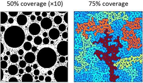
BFO is a target for materials science researchers because of its diverse ferroelectric properties and possible applications in developing technologies such as nonvolatile memory and data storage. At the National Synchrotron Light Source, the researchers discovered that the BFO forms clusters that grow and coalesce into a single layer in an unexpected way. They found that their data agree well with the "interrupted coalescence model" (ICM) of layer growth. This finding was a bit of a surprise, but they propose that the model may be applicable to other layered systems.
"In this system, we saw compact, two-dimensional islands come together efficiently over a range of length scales," said the study's corresponding scientist, University of Vermont physicist Randall Headrick. "However, the kinetics of the growth process behave more like droplets than what we expected to observe, which was single-layer clusters that grow exponentially in time. This growth mode has implications for the structure of interfaces and ferroelectric domains in these materials, which will have an impact on domain switching in devices."
Headrick and his colleagues used a technique called sputter deposition to apply the BFO atoms to the STO surface and "watched" the growth of the BFO layer using x-ray diffraction at NSLS beamline X21. They saw the BFO quickly form islands of varying sizes, with an average size of about 20 nanometers. The small clusters retained their compact shape as they coalesced into bigger clusters. But, this coalescence was kinetically "frozen" when the clusters reached a critical size, leading to the formation of large connected irregularly shaped regions. In the spaces between, smaller islands continued to form and dot the area.
The group confirmed these observations by studying the final layered structure with atomic force microscopy and additional x-ray diffraction measurements.
More information: P. V. Chinta and R. L. Headrick. "Bimodal Island Size Distribution in Heteroepitaxial Growth" Phys. Rev. Lett. 112, 075503 – Published 20 February 2014. journals.aps.org/prl/abstract/ … .112.075503#fulltext
Journal information: Physical Review Letters
Provided by Brookhaven National Laboratory


