Microtechnology: Double-layer capping solves two problems

Continual downsizing of technology means that researchers have to develop ever more ingenious methods of packaging and protecting their tiny devices. Jae-Wung Lee and co-workers at the A*STAR Institute of Microelectronics, Singapore, are at the forefront of efforts to develop safe but functional encasements for microelectromechanical systems (MEMS), such as sensors, switches or radio filters.
"MEMS devices need certain ambient conditions to operate properly and have fragile hanging structures that must be protected," says Lee. "We developed a new thin-film encapsulation (TFE) technique to meet these two requirements."
During TFE, a MEMS device is embedded in a 'sacrificial layer' of one material before adding a 'cap layer' of another type of material. By leaving some access channels in the cap layer, researchers can pipe in a chemical that reacts with and removes the sacrificial layer, leaving the MEMS device in a cavity protected by the cap layer.
Compared with other encasement methods, TFE can be performed cheaply using the same techniques that are used to build MEMS devices, and it produces less bulky packaging. However, previous attempts at TFE have suffered from two problems: depending on the design of the access holes in the cap layer, removing the sacrificial layer can be time consuming, and mass loading can damage moving components, such as resonators, in MEMS devices.
"Solving both these issues simultaneously is difficult because one can become severe when the other is solved," says Lee. "We proposed fabricating the cap layer on two levels."
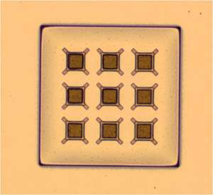
The team's design involves making a grid of square holes in the lower cap layer. A secondary square layer with four legs is deposited on top of each hole, leaving sideways access gaps underneath, rather like a chimney cap. These caps allow access for removing the sacrificial layer while protecting the device beneath from mass loading (see image).
The researchers tested their idea using silicon oxide as the sacrificial layer and aluminum nitride for the cap layers. They were able to remove the silicon oxide using an acid vapor in just 20 minutes, compared to 8 hours for previous designs. The result was a strong, free-standing cap with a 3-micrometer-thick cavity underneath.
Lee and co-workers state that their TFE cavity design could be built using other materials and may find application beyond MEMS, for instance in microbiology. "Electrodes embedded in a TFE cavity could be used to apply electrostatic forces to biomolecules or even act as a microheater," says Lee.
More information: Lee, J.-W., Sharma, J., Singh, N. and Kwong, D.-L. "Development and evaluation of a two-level functional structure for the thin film encapsulation." Journal of Micromechanics and Microengineering 23, 075013 (2013). dx.doi.org/10.1088/0960-1317/23/7/075013
Journal information: Journal of Micromechanics and Microengineering


