Imaging nanoporous metals with beams of electrons provides deep insights into unusual optical properties

Gold is usually thought of as being a shiny metal — however, in its porous form, gold actually appears dull and black. The surfaces of nanoporous gold are rough and the metal loses its shine. Michel Bosman at the A*STAR Institute of Materials Research and Engineering and co-workers have now experimentally demonstrated that the dullness is a consequence of the way incoming light couples to the electrons on the gold surface.
A beam of light hitting metal can cause all of the electrons at the surface to oscillate in unison. If the light is within an appropriate narrow band of wavelengths, it gets absorbed by the surface and creates half-matter hybrid particles known as surface plasmon polaritons (SPPs). Bosman and his team showed that the narrow-band absorption of many SPPs across a surface can combine to give the broadband high-absorption characteristics of nanoporous materials. “Our measurements show that these materials are not black at all when looked at up close; they are actually very colorful,” explains Bosman. “They only appear black to us because we look at them from far away, where over a large area all the different colors have been absorbed.”
These effects caused by the SPPs occur at the sub-micron level. For this reason, conventional optical imaging methods do not offer the resolution necessary to view SPPs directly. In response, the team used imaging techniques based on electron beams. By firing electrons at the surface and measuring the energy that they lose during their interaction with the material, Bosman and his team were able to calculate the energy required to create a SPP, and from this they could infer the wavelength of light that it would absorb.
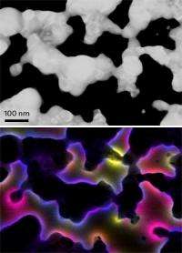
The researchers scanned their electron beam across both gold and silver films, which enabled them to generate a two-dimensional map showing both the wavelength of light absorbed at a particular point as well as the local surface geometry (see image). The varying shape and size of the nanopores gave rise to SPPs that absorb light at a wide range of wavelengths.
The concept could lead to improved power conversion efficiency in photovoltaic devices. “These results show that it is possible to design the color of a gold or silver film,” says Bosman. “It will, for example, be possible to more efficiently absorb the energy of sunlight, by tuning the light absorption of the gold or silver to that of the solar spectrum.”
More information: Bosman, M., et al. Light splitting in nanoporous gold and silver. ACS Nano 6, 319–326 (2012). dx.doi.org/10.1021/nn203600n
Journal information: ACS Nano


