Fujitsu Develops World's First GaN HEMT Able to Cut Power in Standby Mode and Achieve High Output

Fujitsu today announced the development of a new type of gallium nitride (GaN)-based high electron mobility transistor (HEMT) that features a new structure ideal for use in amplifiers for microwave and millimeter-wave transmissions, frequency ranges for which usage is expected to grow.
In a technological first, a novel transistor structure was developed that achieves high output of over 100 watts and enables power to be cut when the transistor is in standby mode. This technological advance will contribute to higher output and lower power consumption in microwave and millimeter-wave transmission amplifiers for high-speed wireless communications.
Details of the new technology were presented at the International Symposium on Compound Semiconductors (ISCS), held in Rust, Germany from September 21 - 24. Certain aspects of research for this new technology were conducted as part of the Research and Development Project for Expansion of Radio Spectrum Resources, sponsored by Japan's Ministry of Internal Affairs and Communications.
As transmission speeds in next-generation wireless communications have become faster, wireless base stations that operate in the microwave frequency range at several gigahertz consume an ever-increasing amount of power. In addition to the fact that the millimeter wave frequency range above 30 GHz has a large amount of available bandwidth that is currently not being used, because it delivers high speed and good directionality, its potential for use in high-speed transmissions is significant. However, due to millimeter-wave frequencies being higher than frequencies for conventional wireless transmissions, it has been difficult to develop amplifiers for practical use that are both compact and economical, and thus the millimeter band is not yet widely used.
Amplifiers based on silicon semiconductors have low breakdown voltages, making it difficult for them to achieve both high frequencies and high power output. As a result, attention has shifted to compound semiconductors, which feature breakdown voltages that are high. For example, the GaN-based semiconductors have high innate breakdown voltages, making them appropriate for high-output applications. The development of high-output power amplifiers would make microwave and millimeter-wave transmissions possible, thereby enabling their use in high-speed wireless communications.
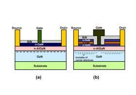
Amplifiers based on previous compound semiconductors required a negative voltage to be added to the gate electrode even when the circuit was in standby mode, resulting in the problem of high power consumption. This is attributable to the fact that the transistors being used require negative voltage to be continuously applied to the circuit-power cutoff switch in order to turn off the electron flow (see Figure 1a). Thus far, no compound semiconductor transistor had been able to both generate 100 W of power output and cut power without requiring the addition of negative voltage. In addition, because the design of the control circuits used in previous transistors has been very complex, they required more power to be consumed.
Figure 1b shows the structure of Fujitsu's newly-developed GaN HEMT transistor, the world's first that does not require a negative voltage to turn off the circuit's power. Key features of this structure include the following:
-- The addition of an aluminum nitride (AlN) layer on top of the n-type GaN layer increases the density of carrier electrons when on, making this design naturally amenable to higher output.
-- The design of the gate electrode, which was formed after removing the AlN layer, decreases the density of carrier electrons around the region below the gate electrode, preventing current from flowing even in the absence of a negative voltage.
-- If the topmost layer is made of AlN, this results in a micro-cracked surface, which degrades the breakdown voltage. This issue has been resolved by adding a n-type GAN-based layer above the AlN layer, resulting in a three-layer cap structure that improves the surface roughness and also raises output and reliability.
The newly developed three-layer cap structure obviates the need for a negative voltage across the gate electrode and results in a GaN HEMT that allows power to be cut during standby. Fujitsu also verified that the addition of an AlN layer increased the volume of electrons transmitted by 60% (Figure 1b). This results in the characteristic of being able to sustain high current densities when on, and power to be cut when on standby.
The three-layer structure that covers the AlN layer with n-type GaN reduces surface roughness, permitting breakdown voltages that are high and exceeding 300 volts, thereby resulting in an unprecedented combination of achieving high current densities and high breakdown voltages. This enables high-efficiency power amplification with low resistance and low power consumption. Implementation of this new transistor structure eliminates the need for power during standby, and has realized output exceeding 100 W, the first time that both have been achieved simultaneously.
Provided by Fujitsu


