IMEC advancing state-of-the-art in FinFETs

At this week’s VLSI Symposium, IMEC presents significant progress in the manufacturability, circuit performance and reliability of FinFETs. The results advance FinFET process technology towards being a candidate for the 32nm node and beyond.
FinFETs are a promising approach to address short-channel effects and leakage issues when scaling CMOS towards the 32nm node and beyond. Doping fluctuations in nano-scale planar devices are one of the several concerns in further scaling, while FinFETs have the potential of being able to operate without channel dopants.
IMEC has improved its process to yield reproducible FinFETs with fin widths down to 5nm and high aspect ratio using 193nm immersion lithography and dry etching. By using these ultra-thin body devices, the need of channel doping is eliminated. This results in reduced parametric spread due to dopant fluctuations together with reduced junction leakage.
Analyzing various circuit topologies, IMEC demonstrates experimentally that the performance of FinFET circuits is superior to bulk CMOS circuits and satisfies future digital library requirements. A ring oscillator has been realized with metal gates and un-doped fins showing an inverter delay of 13.9ps at a 1.0V supply voltage and 1.9nA off current. This best low-power performance of FinFETs ever reported results from the undoped channels and improved subthreshold characteristics.
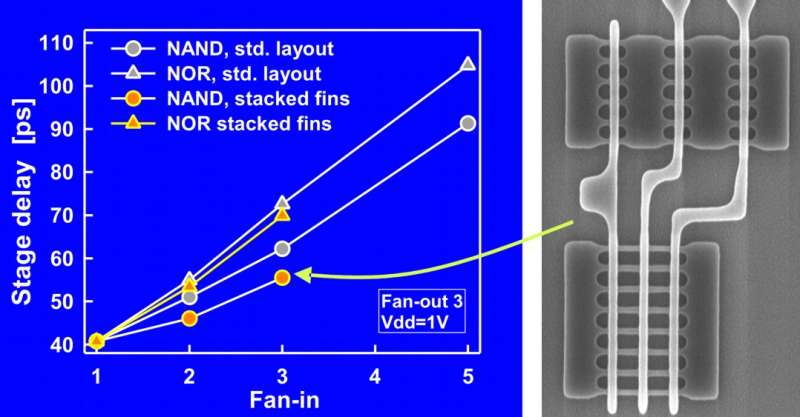
Next to the excellent inverter delay, FinFETs provide an extra performance benefit due to their excellent stacked device performance. They allow realizing higher stack heights whereby the same functionality can be implemented with less logic gates resulting in additional area reduction. The potential of FinFETs for large-scale integration has also been demonstrated. To this end, SRAM cells and data path demonstrators with low standby current and good low operating power performance were realized.
The reliability characteristics, both NBTI (negative bias temperature instability) and PBTI (positive bias temperature instability), of the FinFETs have been significantly improved by dielectric passivation based on introducing fluorine into the metal/Hf-based gate stack during gate etching. To this end, IMEC developed a novel, effective and cost-efficient method that requires no extra processing step.
"Although the performance benefits of FinFETs have been recognized for many years, several bottlenecks have to be overcome to bring FinFET technology to manufacturing. These advances have reduced the gap for FinFETs to become a manufacturing technology," said Luc Van den hove, COO IMEC.
These results were obtained in collaboration with IMEC’s (sub-)32nm CMOS research partners: Infineon, Qimonda, Intel, Micron, NXP, Panasonic, Samsung, STMicroelectronics, Texas Instruments, TSMC and Elpida.
Source: IMEC


