February 17, 2015 feature
Nano switch could store memory using coordinated 'dance' of atoms
Lisa Zyga
contributing writer

(Phys.org) —In one of the tiniest switches ever made, five atoms appear to "dance" around each other in a complex choreographic sequence, with their final arrangement corresponding to one of two stable states. This concerted motion of multiple atoms is unlike that in other nano switches, which typically involve movement of only a single atom or molecule. The motion of multiple atoms gives the switch a major advantage: due to its stability, it is one of the few atomic-scale switches capable of operating at room temperature instead of cryogenic temperatures.
The researchers, Eiichi Inami, et al., at Osaka University and Japan's National Institute for Materials Science, have published their paper on the room-temperature, atomic-scale switching device in a recent issue of Nature Communications.
Nano switches are part of the larger goal of developing miniaturized electronic components, where single atoms and molecules serve as the tiniest building blocks physically possible. Scientists use the tips of microscope, such as those on scanning tunneling microscopes (STMs) and atomic force microscopes (AFMs), to apply single-electron pulses that move individual atoms and molecules in a controlled way.
Although many atomic-scale switches have been demonstrated using these microscopes, most switches operate only at cryogenic temperatures. This is because heat causes uncontrollable processes that interfere with the atomic movement, causing switching at undesired times.
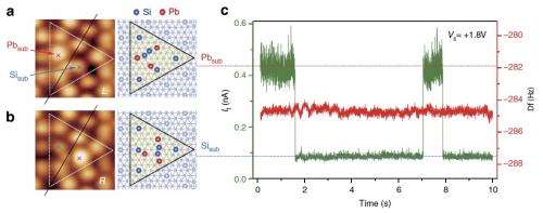
To make a stable, room-temperature, atomic-scale switch, the researchers in the new study used a microscope tip to collect lead (Pb) atoms one by one and place them in a confined half-unit cell on a silicon (Si) surface. Although individual Pb atoms exhibit "thermal hopping," the researchers found that a cluster of three Pb atoms (Pb3) is thermally stable at room temperature due to its larger size, yet still small enough to respond to the electric current from the microscope tip.
As shown in experiments and modeling, each confined cell has two possible stable arrangements of Pb3 and Si atoms. To switch between states, a microscope tip is scanned over a specific Pb or Si atom, which triggers a complex motion involving two Pb and three Si atoms. The researchers describe this motion as a chiral inversion, meaning that the two stable states are mirror images of one another after being translated and rotated. This "chiral switch" can be repeatedly switched back and forth between the two states, which correspond to high and low electric currents.
"Our nanostructure control can add a function to a cluster," Inami explained to Phys.org. "Since a cluster—an aggregation of a few to a few hundred atoms—sometimes exhibits superior properties with particular size and composition, controlling cluster structure is one promising approach to realizing atomic-scale devices. Our technique enables proper adjustment of cluster size and constituent atoms with single-atom accuracy. Using this method, we precisely controlled the structural stability of a cluster so that it functions as a room-temperature switch."
Overall, the switch demonstrates that Pb3 can potentially function as a basic unit of memory. To realize a complete memory device, several cells need to be integrated into a periodic, well-ordered array. The scientists suggest that self-assembly processes could be used to construct such a memory device, and may ultimately lead to ultra-high-density recording and reading of information at room temperature.
"We think that this switch could become a powerful tool for basic research," Inami said. "For example, the switch has an interesting feature, that the switching occurs between opposite chirality, resulting in a chiral switch. Chiral technology aimed at the synthesis of 'enantiopure compounds' [which have just one chiral form] provides ultimate control of chemical reactions and has been a target in physics, chemistry, biology and pharmacology. Our approach can construct switchable chiral motifs at atomically precise positions, such as the creation of homochiral domains/clusters and the allocation of chiral species near some reactive elements. These may provide a clue to basically understand chiral selective reactions from a microscopic view."
In the future, the researchers plan to apply their technique to designing other nanoscale devices.
"One of our future plans is to explore other new functionalities hidden in several clusters," Inami said. "Our technique to construct atomically defined clusters is widely applicable to various elements. This motivates us to create a variety of clusters with different functionalities and systematically embed them into desired nanoscale regions. We believe this opens up novel nanofabrication to achieve atomic-scale integrated electronics."
Written for you by our author Lisa Zyga—this article is the result of careful human work. We rely on readers like you to keep independent science journalism alive. If this reporting matters to you, please consider a donation (especially monthly). You'll get an ad-free account as a thank-you.
Publication details
Eiichi Inami, et al. "Room-temperature-concerted switch made of a binary atom cluster." Nature Communications. DOI: 10.1038/ncomms7231
Journal information: Nature Communications
© 2015 Phys.org


