Manipulating magnetic field effects in organic semiconductors

Changing the polarity of the magnetic field response of a material one thousandth the width of a human hair may seem like the stuff of science fiction, but that's exactly what's happening at NIST.
Researchers led by Curt Richter and Hyuk-Jae Jang of PML's Semiconductor and Dimensional Metrology Division have found a way to change the magnetoresistance of a thin (≈ 100 nm) organic semiconducting material by pairing it with an even thinner layer—a self-assembled monolayer (SAM)—to alter its characteristics. By demonstrating that this kind of fine tuning is both straightforward and repeatable, the researchers have opened up an unprecedented level of control over materials that hold huge promise for next-generation technologies.
Magnetoresistance is the change of electrical resistivity under magnetic fields. Magnetoresistance has been widely used in commercial applications such as computer hard disk storage and on-chip sensors, especially after the 2007 Nobel Prize winning discovery of giant magnetoresistance in metallic systems.
Organic semiconductors are regarded as potentially revolutionary materials in many areas of device technology. These materials have unique electronic properties and functions that can be tailored by chemical synthesis and molecular engineering. In addition, they are expected to provide lower cost, lighter, and more mechanically flexible electronic assemblies than current inorganic-based technology. But there is much to be learned about the properties of these materials, which can behave differently based on changes in magnetic field, temperature, film thickness, and many other factors.
Manipulation of electronic and optoelectronic properties of organic materials by magnetic fields can impact electronic and spintronic technology – by affecting the functionality of various organic-based devices such as light-emitting diodes, photovoltaics, and field-effect transistors, and by enabling the invention of novel spintronic devices such as flexible memory storage.
Using a self-assembled monolayer to influence the behavior of a device made of organic semiconductors is not a new idea. Using one to influence the magnetic-field effect, however, is a unique idea born at NIST.

"Non-magnetic organic materials can show a magnetoresistance," Jang explains. "Researchers found that, in certain cases in certain systems, the polarity of the resistance can change. So, depending on the film thickness, whether you inject two different charge carriers or one carrier, if you change the temperature, or sometimes if you change the voltage, you may change the polarity of the magnetoresistance. We thought that if we put down a self-assembled monolayer before putting down organic materials, maybe it will change some microstructure inside of the organic film so that we can alter the polarity of the magnetoresistance in the film. That's how it started."
It turns out, adding that monolayer changed the structure of the material profoundly.
Richter elaborates: "We thought that adding a self-assembled monolayer would change things. We didn't necessarily think it would change things the way it did. We thought we were going to tune the energetics of this interface when instead we changed the processing to make the device; we changed the physical morphology."
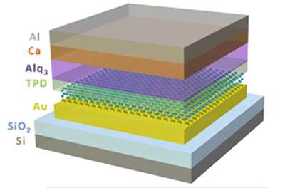
In their experiment, Richter and Jang created a bilayer system, using a 100 nm layer of Alq3 (tris-(8-hydroxyquinoline) aluminum)—an organic semiconductor—and a 10 nm layer of TPD [N, N'Bis(3-methylphenyl)-N, N'-diphenylbenzidine]. A metal electrode, Au, was coated with a fluorinated SAM and placed beneath the TPD layer. The system was finalized with the deposition of 20 nm of Ca followed by 100 nm of Al (see figure below). Richter and Jang produced 20 of these systems and 20 control systems that did not include the SAMs.
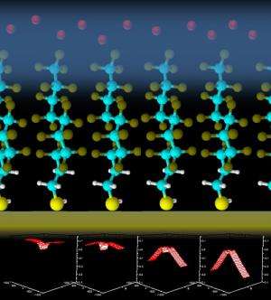
The devices were characterized using various tools including magnetoresistance measurement and impedance spectroscopy. The results were consistence throughout all of the samples: the control samples (without the SAM) had a negative polarity of magnetoresistance; the samples with the SAM showed a positive magnetoresistance. The data confirm that the behavior of the electrons and holes at the interface of Au and TPD layers is altered by the presence of the SAM, which causes charge trapping due to its rough surface after it is applied to the Au. This effect is carried over to the TPD/Alq3 interface as well.

Changes at the interface of a device can profoundly affect the way the device performs: "The way the energy of the various materials lines up at the interface is critical to the performance of these diodes or light emitters," Richter explains. "You can sort of tune that energy alignment by putting the right self-assembled monolayer in there. We also found that if we used this bilayer device, we could tune this magnetoresistance by supplying a bias voltage. We thought we were going to tune the energetics of this interface when instead we changed the processing to make the device; we changed the physical morphology."
Richter anticipates that this metrology breakthrough can have enormous impact, most immediately on organic light emitting diodes, which are structurally very similar to the devices Richter and Jang tested in this study.
"With this new understanding, the hope is that we could perhaps, by getting the right structure and applying the magnetic field, improve the efficiency and performance of organic light emitting diodes," Richter explains.
Further down the road, Richter and Jang hope to apply the technique to perform magnetic field measurements on photovoltaic structures to see if they can better understand and improve organic photovoltaics.
More information: Jang et al., "Interface Engineering to Control Magnetic Field Effects on the Electrical Resistance of Organic-Based Devices," ACS Nano, Jun. 26, 2014. DOI: 10.1021/nn502199z
Journal information: ACS Nano
Provided by National Institute of Standards and Technology


