Bursting through the silicon barrier: Developing carbon-based nanoelectronics with graphene

(Phys.org)—On the road towards creating smaller and smaller electronic devices, silicon blocks the way by limiting the smallness of the electronic components that can be constructed with it. A promising way forward has been found by using carbon instead and its study has resulted in a rapidly growing field. In a work published in ACS Nano, using tools including those found at the Synchrotron Radiation Center, scientists have developed a process for making a never-before-seen, atomically thin, composite material containing ordered layers of graphene and nanocrystals of graphene monoxide.
Graphene, composed of an atomically thin layer of carbon, does not by itself have the necessary properties that lend itself for use in modern nanoelectronics. To achieve this, other elements need to be added to the mix. When oxygen is added chemically to graphene, for example, a property called the band-gap is created. The band-gap determines the electrical conductivity of a material, an important factor in creating useful electronic devices. However, at this stage, the mix is a disorganized arrangement of atoms, and results in poor electronic properties, including the band-gap. Because of this it can only be used in basic electronic devices such as supercapacitors, sensors, and flexible transparent conductive electrodes.
In this publication researchers describe a method for annealing (heating) the graphene and oxygen mix resulting in a previously unobserved atomic structure. It is comprised of layers of oxygen poor graphene sandwiched between layers of oxygen rich graphene (graphene oxide).
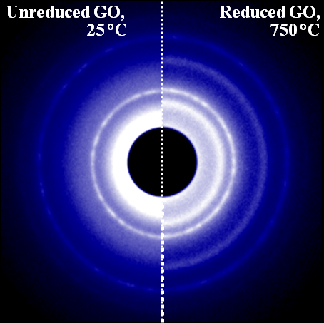
In the image, the number of rings corresponds to the complexity of the different structures in the Graphene-Oxide (G-O) compound. The left side of the image corresponds to the G-O compound before annealing (heating). The right side of the image, corresponding to the compound after annealing, shows additional rings indicating a more complex and ordered structure.
Scientists determined that the new carbon based structure shows promise allowing them to tailor it creating, for example, ideal "band gaps" for use in nanoelectronic devices such as sensors, transistors, and optoelectronic devices.
Provided by University of Wisconsin-Madison


.jpg)


