Researcher charts quantum signatures of electronic transport in graphene

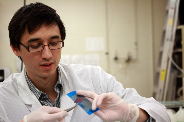
Over the last seven years, Javier Sanchez-Yamagishi has built several hundred nanoscale stacked graphene systems to study their electronic properties. "What interests me a lot is that the properties of this combined system depend sensitively on the relative alignment between them," he says.
Sanchez-Yamagishi, who received his PhD in January, is now a postdoc in Associate Professor Pablo Jarillo-Herrero's group. He assembles sandwiches of graphene and boron nitride with various horizontal orientations. "The tricks we would use were making cleaner devices, cooling them down to low temperatures and applying very large magnetic fields to them," says Sanchez-Yamagishi, who carried out measurements at the National High Magnetic Field Laboratory in Tallahassee, Florida. The lab features the largest continuous magnet in the world, 45 Tesla, which is about 10,000 times the strength of a refrigerator magnet.
Sanchez-Yamagishi was a lead co-author of a 2014 paper in Nature that showed that having a component of the applied magnetic field in the graphene plane forced electrons at the edge of graphene to move in opposite directions based on their spins. Lead co-authors were postdoc Benjamin M. Hunt and Pappalardo Fellow Andrea Young, both from MIT Physics Professor Raymond C. Ashoori's group. The paper was the culmination of two years' work, Sanchez-Yamagishi says.
"We were trying to realize some interesting quantum states in the graphene. It's called a quantum spin Hall state," Sanchez-Yamagishi explains. That would have applications in quantum computing, an area of interest to the group because Jarillo-Herrero is a researcher in the National Science Foundation-funded Center for Integrated Quantum Materials.
Sanchez-Yamagishi also was a co-author of a 2013 Science paper in which Jarillo-Herrero, Ashoori, and collaborators demonstrated that a certain alignment of layered graphene and hexagonal boron nitride created a unique bandgap in graphene, which could be a precursor to developing the material for functional transistors. Sanchez-Yamagishi's co-authors again included Young, now assistant professor at the University of California at Santa Barbara, and Hunt, who will join the faculty of the Carnegie Mellon physics department this fall.

Hofstadter's butterfly
Graphene and boron nitride layers each have atoms arranged in a hexagonal, or six-sided, pattern. When the lattice arrangement of graphene and hexagonal boron nitride layers are closely aligned, and the samples are exposed to a large out-of-plane magnetic field, they exhibit electronic energy levels that are called "Hofstadter's butterfly," because when they are plotted on a graph it resembles a butterfly. What excites physicists is that this butterfly is one of the rare examples of a fractal pattern in quantum physics. "These are physics that only come into [play] because the electrons are very small and we make them very cold. So quantum physics takes a role and it is very different, shockingly different," Sanchez-Yamagishi says.
"In addition to the Hofstadter butterfly result, the same devices were also the first to show a bandgap in graphene. Jarillo-Herrero says, "What was very unexpected was we showed that graphene, which usually conducts very well, under the conditions of that experiment with a very low angle of rotation between the graphene and the HBN, became an insulator. It didn't conduct at all. That was a behavior which was unexpected and [it] is still. Theorists are still trying to understand why. At a quantitative level, it's not understood yet. So it's understood qualitatively, but not quantitatively."
Fortunate discovery
The peculiar electronic behavior of graphene comes from its molecular structure, which is like a honeycomb or chicken-wire-shaped lattice of carbon atoms. When these honeycomb structures are stacked on top of each other, if they are out of alignment, they create a so-called moire pattern, which varies with rotation of the layers with respect to each other. "What happened was that by accident, we got these samples that displayed this Hofstadter physics. So that was not our original intention," Sanchez-Yamagishi explains. "To see Hofstadter physics, the graphene has to be very closely aligned to hexagonal boron nitride. When it's closely aligned, you have a very large superlattice, and then the physics gets strongly affected, and that's why we were able to observe this Hofstadter physics," he says. To put it another way, he says, "When they are misaligned, the moire is very small, and when the moire is small, it has very little effect on the physics of the electron. But when they're aligned, the more they are aligned, the larger the moire and the stronger the effect on the electrons, and so basically to see this type of Hofstadter physics you need a big moire."
While this honeycomb structure exists in graphite, a familiar bulk form of carbon, its special properties only show when layers of graphene just one to few atoms thick are separated from the graphite. "Graphene conducts electricity better than graphite. It conducts better than silver or gold," Sanchez-Yamagishi says.
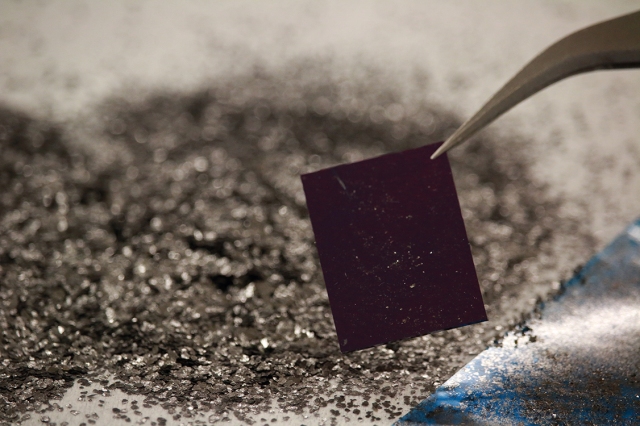
Sanchez-Yamagishi built a machine in the lab that stacks extremely thin layers of graphene and similar materials. When two layers of graphene are misaligned, they are called twisted bilayer graphene. "In graphite, normally all the layers are aligned with each other; electrons get slowed down," he explains. It turns out that if two layers of graphene are stacked in alignment, electrons traveling within a layer are slowed down in the same way. But with graphene, if the layers stacked on top of each other are misaligned, they act as if one layer doesn't really feel the other layer. "You can put it right on top of each other, they actually remain decoupled from each other, and it can still conduct electricity basically as well as if it was still a single sheet of graphene," he says. "If they are misaligned, then the electron in one layer does not get affected by the other layers and zips along quickly."
While the twist, or rotation out of alignment, can enhance electron flow through individual layers, it has the opposite effect on electrons moving between layers. "Even though they are right on top of each other, atoms apart, if you twist them, then the electrons cannot actually go from one layer to the other just by themselves. They need help from other elements in the system. So you can put them right on top of each other, they're actually not electrically connected. It's related to this moire pattern. It's because of the twisting between the two layers that decouples them in this way," Sanchez-Yamagishi says.
Learning curve
One of the first graduate students to join Jarillo-Herrero's group in 2008, Sanchez-Yamagishi, 28, says he has grown from initially spending months to make good quality graphene to now making very intricate graphene devices and combining then with other materials. Gold contacts send current through the graphene to measure its electrical properties. Often, graphene shapes used in test devices are irregularly shaped since that is how they come off the natural graphite material. The graphite is rubbed on a sheet of silicon and lifted off with special tape to create thin layers of graphene. Maximizing the amount of graphene that can be used for a device takes priority over making it look nice, Sanchez-Yamagishi says. "We're trying to push the technology to the highest level, so we're kind of relying on the tail end of the distribution here. We want to get that tail end, the ones that are abnormally good performing, because we want to demonstrate the physics," he says. "In the end, we weed out the ones that are not high quality, and we keep the ones that are the best."
The studies are conducted at low temperatures, about 4 kelvins—though some are even colder, measured in millikelvins. "A big focus of our lab is just studying electricity in the form of how electrons move around and so to do that we first want to cool it down to low temperatures where all we see is how the electron behaves by itself primarily, and then we can worry about making things more complicated as well," Sanchez-Yamagishi explains. He is also mentoring current graduate students Yuan Cao and Jason Luo.
In September, Sanchez-Yamagishi will begin a two-year postdoctoral fellowship at the Harvard University Quantum Optics Center, where he'll work on nitrogen-vacancy centers in diamond under lead researcher Mikhail Lukin. "My background is electronics in graphene, so the idea is to combine electrons in graphene with photons in diamonds," he says. He hopes eventually to become a physics professor.
Journal information: Nature
Provided by Massachusetts Institute of Technology
This story is republished courtesy of MIT News (web.mit.edu/newsoffice/), a popular site that covers news about MIT research, innovation and teaching.


