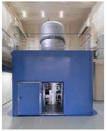
Atomic-resolution holography electron microscope with the world's highest point resolution

Hitachi today announced that it has developed an atomic-resolution holography electron microscope accelerated at a 1.2-megavolt ("MV") under the government-sponsored FIRST Program project named "Development and Application of an Atomic-resolution Holography Electron Microscope", and has achieved the world's highest point resolution of 43 picometers ("pm"), i.e., 43 trillionths of a meter. With its ability to measure electromagnetic fields at the atomic resolution, the developed microscope will contribute to the advancement of fundamental sciences by supporting the development of cutting-edge functional materials, through elucidating quantum phenomena that cause the functions and properties of high-performance materials, such as magnets, batteries, and superconductors.
In recent years, significant progress has been made in the development of technologies that enable the measurement of electromagnetic fields causing the functions and properties in and around materials at atomic resolutions. For example, materials for magnets must have not only high magnetic performance at room temperatures, but they are also required to be usable under high temperatures and high magnetic fields. To develop such magnetic materials, the following procedures are required: evaluation of the atomic arrangements in those materials, determination of their magnetic properties, and acquisition of guiding principles for optimum material compositions and arrangements and manufacturing methods. For these purposes, electron microscopes with higher resolutions have been developed.
In 2000, Hitachi in collaboration with the University of Tokyo developed an 1-MV holography electron microscope financially supported by CREST program of the Japan Science and Technology Agency (JST) and achieved point resolution of 120 pm making it possible to measure electromagnetic fields in the microscopic region.
Furthermore, from 2006 to 2008, Hitachi participated in the MEXT Leading Project and developed a technology for creating high-brightness monochromatic electron beams, resulting in the improvement of the resolution capability of electron microscopes.
On the basis of these technologies, since March 2010, Hitachi has been developing an "atomic-resolution holography electron microscope" that can visualize electromagnetic fields at the atomic level with the support of the FIRST program. To improve the resolution of the microscope to the utmost limit, the following technical developments were made including an increase in the acceleration voltage to 1.2 MV resulting in decrease in electron beam wavelength and installation of a spherical-aberration corrector. The main features of the technologies developed in the current project are described below.
(1) World's first installation of a spherical-aberration corrector in an ultra-high-voltage electron microscope
In an optical microscope, spherical aberrations are corrected by combining convex and concave lenses to eliminate focus blurring and then magnified images of specimen structures are observed. In an electron microscope, however, a concave electron lens system has been difficult to manufacture so that improvement of the resolution limit has been prevented by spherical aberration. Recently, although spherical aberration correctors have been developed by combining electron lenses in a sophisticated structure and have been installed in conventional electron microscopes, their installation in an ultra-high-voltage electron microscope requires high stability of the microscope system.

In the current project, a 1.2-MV electron beam with suppressed energy dispersions and a high-stability field-emission electron gun have been achieved successfully, and they made it possible to improve the stability of the electron microscope system. As a result, for the first time in the world, a spherical aberration corrector could be installed in an ultra-high-voltage electron microscope.
(2) A 1.2-MeV electron beam with suppressed energy dispersion
To obtain high resolution, acceleration of electron beams by stabilized voltage is essential, because dispersions of the electron beam energy result in focus blurring. To realize the voltage stability, the following technologies were developed: low-noise resistors with low temperature coefficient, high-voltage cables with noise-filtering capability, and high-voltage control circuitry with high stability. Combining these technologies, an ultra-high voltage power-supply system was completed with 3×10⁻⁷ stability, which is 70% more stable than that of the 1 MV electron microscope. These developments realized electron beams having a high energy of 1.2 MeV while having an energy dispersion reduced down to 0.54 eV.
(3) An electron gun emitting high brightness electron beams with long-term stability
In field-emission electron guns in conventional electron microscopes, electron beam current is decreased right after electron begins to be emitted, if the extract voltage is constant. Therefore it is required to raise the extract voltage two or three times a day in practical operations. Because electron beam trajectories change slightly with extract voltage raise, obtaining the full effects of the spherical-aberration corrector under the optimum condition becomes difficult. The newly developed electron gun, however, has a vacuum 100 times better than conventional field emission guns, namely 3×10⁻¹⁰ Pa. Therefore, without raising the extract voltage stable electron beam can be emitted stably after the start of electron emission for more than ten hours. As a result, best performance of emitted electron beams can be maintained for a full-day observation without having to re-adjust the conditions of the spherical-aberration corrector.
(4) Development of facility technologies to eliminate degradation factors of resolution
To achieve observations at the atomic level, external disturbances, such as vibrations, noises, and ambient magnetic fields, to electron beams and specimens must be minimized to the utmost limit. For these purposes, a robust building for housing the electron microscope was constructed. In particular, acoustic-absorption materials were placed on the interior walls of the building to reduce sound noises, and precise-room-temperature control units were installed; moreover, the electron microscope was covered with magnetic-shielding "permalloy" to reduce ambient magnetic field effects.
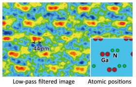
For performance evaluation of the developed electron microscope, its information transfer, indicating a specimen fine structures transfer capability to its camera, was measured by using a tungsten single crystal. The results indicated that the electron microscope can transfer crystal-structure information of a world-finest resolution of 43 pm under the corrected spherical aberration condition. Furthermore, gallium-nitride (GaN) single crystal observation showed the atomic resolution of 44 pm, i.e., isolated gallium atoms with a spacing of 44 pm were clearly shown (see Figure 2). This result demonstrates that the developed electron microscope can visualize specimen structures and electromagnetic fields at the atomic level.
The present FIRST Program has been jointly conducted by three institutions: Hitachi, Ltd. has been engaged in the development of holography electron microscope, RIKEN has been engaged in development of application technologies of electron microscopes and their application to materials science and technology, and Japan Science and Technology Corporation has engaged in supporting managerial tasks. In particular, at RIKEN, scientific achievements in the following three areas were realized: three-dimensional (3D) observations of internal electric potentials in and around materials, fine magnetic behavior observations of microscopic region within magnets, and observations of magnetic vortices called "skyrmions", promising candidates for memory devices with ultra-low power consumption.
Ongoing forward, Hitachi will collaborate with world-first-class research institutes including RIKEN, and will use the developed holography electron microscope to study quantum phenomena of emergent materials by measuring their electric and magnetic fields at the atomic scale, for example, high-performance magnets, large-capacity rechargeable batteries, low-power-consumption memory devices, and high-temperature superconductors. And in doing so, Hitachi will contribute to the advancement of quantum mechanics, condensed-matter physics, materials science and technology, and other fields while developing new materials that will support a sustainable society.
The development project has been funded by Japan Society for Promotion of Science, an incorporated administrative agency. The results of the project will be published online at Applied Physics Letters today.
More information: Tetsuya Akashi, Yoshio Takahashi, Toshiaki Tanigaki, Tomokazu Shimakura, Takeshi Kawasaki, Tadao Furutsu, Hiroyuki Shinada, Heiko Müller, Maximilian Haider, Nobuyuki Osakabe, and Akira Tonomura "Aberration corrected 1.2-MV cold field-emission transmission electron microscope with a sub-50-pm resolution", Applied Physics Letters, 2015, DOI: 10.1063/1.4908175
Journal information: Applied Physics Letters
Provided by Hitachi


