Planting imperfections at specific spots within diamond lattice could advance quantum computing

By carefully controlling the position of an atomic-scale diamond defect within a volume smaller than what some viruses would fill, researchers have cleared a path toward better quantum computers and nanoscale sensors. They describe their technique in a paper published in the journal Applied Physics Letters, from AIP Publishing.
David Awschalom, a physicist at the Institute for Molecular Engineering at the University of Chicago, and his colleagues study a technologically useful diamond defect called a nitrogen vacancy (NV) center. NV centers consist of a nitrogen atom adjacent to a vacant spot that replaces two carbon atoms in the diamond crystal, leaving an unpaired electron. Researchers can use a property of the unpaired electron known as its spin to store and transmit quantum information at room temperature.
Qubits and Quantum Sensors
NV centers are attractive candidates for qubits, the quantum equivalent of a classical computing bit. A single NV center can also be used for completely different applications, such as measuring temperature, as well as to image electric and magnetic fields on the nanometer-scale by placing it at the tip of a diamond-based scanning probe.
A primary obstacle to further exploiting NV centers for practical quantum computing and nanoscale sensing devices lies in the difficulty of placing the centers within what Awschalom calls the functional "sweet spots" of the devices. Another challenge is increasing the NV center density without sacrificing their spin lifetimes, which must remain long in order to extract the most useful information from the system.
Awschalom and his colleagues have developed a new way to create NV centers that could help overcome both these challenges.
That's the Spot
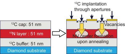
The key to the team's new approach is to create the nitrogen and vacancy defects separately, Awschalom said. First, the team grew a layer of nitrogen-doped crystal within a diamond film. The researchers kept the nitrogen layer extremely thin by reducing the growth rate of the film to approximately 8 nanometers/hour. The nanometer-scale nitrogen-doped layer constrains the possible location of the NV centers in the depth direction.

Secondly, the researchers created a mask to cover the film, leaving only pinprick holes. They blasted carbon ions through the holes to create vacancies and heated the diamond to make the vacancies mobile within the crystal. NV centers could form in the nitrogen-doped layer below where the holes were placed.
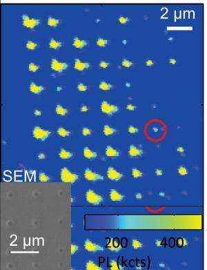
Using this approach the team successfully localized NV centers within a cavity approximately 180 nanometers across—a volume small enough to be compatible with many diamond-based nanostructures used in sensing devices and experimental quantum information systems.
The localized NV centers could also hold a specific spin for longer than 300 microseconds. This so-called spin coherence time was an order of magnitude better than that achieved by other 3-D localization methods. The longer spin lifetime means the NV centers can detect smaller magnetic signals and hold quantum information for longer.
One of the team's goals for using their new technique is to measure the nuclear spins of hydrogen atoms – one of the tiniest magnetic signals – within a biological molecule. The research could reveal new insights into how important biological functions like photosynthesis work. "Our research impacts diverse fields of science and technology," Awschalom said. "Technological advancements always open new avenues of scientific research."
More information: "Three-dimensional localization of spins in diamond using 12C implantation," by Kenichi Ohno, F. Joseph Heremans, Charles F. de las Casas, Bryan A. Myers, Benjamín J. Alemán, Ania C. Bleszynski Jayich, and David D. Awschalom, Applied Physics Letters August 5, 2014. DOI: 10.1063/1.4890613 . scitation.aip.org/content/aip/ … /5/10.1063/1.4890613
Journal information: Applied Physics Letters
Provided by American Institute of Physics


