July 1, 2013 feature
Hybrid nanostructure with extreme light absorption looks promising for photovoltaics

(Phys.org) —In photovoltaics, there is generally a trade-off in terms of semiconductor thickness, with thicker semiconductors offering better photon absorption and thinner ones offering higher charge carrier extraction efficiency. In recent years, scientists have begun investigating semiconductor nanowire solar cells, which tackle this tradeoff through morphology-dependent resonances that significantly enhance the absorption compared to a planar film.
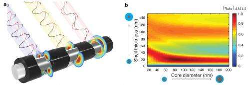
Now, somewhat counterintuitively, scientists have theoretically found that thin semiconductor films wrapped around metal nanowires have substantially better light absorption properties than solid semiconducting nanowires, despite the fact that they use less semiconducting material. At the same time, the metal core acts as a contact to efficiently extract charge carriers. By confronting the semiconductor thickness trade-off and offering exceptional performance, the nanostructures might become ideal building blocks for inexpensive photovoltaic and solar fuel applications.
A paper on the new devices by Sander A. Mann and Erik C. Garnett at the Center for Nanophotonics at FOM Institute AMOLF in Amsterdam, The Netherlands, will be published in a future issue of Nano Letters.
"The greatest significance to our work is that we provide a design for nanowire building blocks that incorporates both excellent light trapping properties and a local metal electrode contact (for current extraction)," Garnett told Phys.org. "Silver nanowire networks have already been used as high performance transparent electrodes and we expect that by coating them with thin semiconducting shells we will be able to make high-efficiency solar cells using cheap materials. It has now been observed in a number of papers that nanostructuring a material can increase light absorption even while using less semiconductor material. However, this paper takes the next step and starts thinking about how to design such structures with integrated electrical contacts."
One of the biggest advantages of the design is that it uses very thin semiconducting films while at the same time providing very good light absorption. As mentioned, thick semiconductor layers are needed for good light absorption, but high-quality semiconductor is very costly. This new core-shell geometry opens up a pathway to using cheap, abundant, and environmentally friendly semiconductors that previously were of too low quality for good charge extraction.
In semiconductor objects smaller than the wavelength of light, as is the case with most nanowires for photovoltaic purposes, the optical properties are determined primarily by resonances. These resonances enhance absorption the most when they are critically coupled: the loss rates due to absorption in the semiconductor and due to radiative leakage (light escaping the nanowire before being absorbed) are equal. This is often the case near the band gap of the material, where absorption is weak, which leads to the highly counterintuitive result that absorption in the nanowire actually increases when the absorption coefficient decreases.
As the scientists explain, in the core-shell geometry, extreme light absorption arises from increasing the number and strength of these resonances. Whereas in horizontal nanowires resonances are always spectrally separated (at different wavelengths), in the core-shell geometry they can overlap. Furthermore, horizontal solid seminconductor nanowires are very polarization-sensitive, but this is undesirable as light from the sun is unpolarized. The core-shell geometry gets rid of this polarization dependence by aligning resonances in both polarizations simultaneously.
Overall, by demonstrating that excellent light absorption can be achieved in very thin semiconductor layers, this hybrid nanostructure offers an exciting new path toward realizing inexpensive solar technologies based on abundant and environmentally friendly semiconductors. The researchers plan to fabricate prototypes of the devices soon.
"Our immediate plans are to make both single-nanowire and array solar cells based on these core-shell building blocks to verify our calculations experimentally," Garnett said.
More information: Sander A. Mann and Erik C. Garnett. "Extreme Light Absorption in Thin Semiconductor Films Wrapped around Metal Nanowires." Nano Letters. DOI: 10.1021/nl401179h
Journal information: Nano Letters
© 2013 Phys.org. All rights reserved.


