Simpler fabrication of nanogaps

Plasmons, which are density waves of electrons, are of great interest to pure and applied scientists because of their novel properties, and because of their application to sensing and photonic technologies. These applications are possible because plasmons are sensitive to surface properties, and allow for the concentration of electric fields into small volumes. Fabricating the intricate nanostructures necessary to support plasmons, however, has proved a challenge. Now a straightforward fabrication technique, capable of generating plasmon-supporting nanogap structures over large areas, has been demonstrated by Wakana Kubo and Shigenori Fujikawa from the RIKEN Innovation Center, Wako, and the Japan Science and Technology Agency.
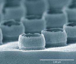
The researchers fabricated many copies of a structure consisting of two nested vertical gold cylinders, with the cylinders spaced apart by tens of nanometers. This structure, called a ‘double nanopillar’, was designed to support a highly concentrated electric field in the gap between the cylinders, in response to illumination with light. When the gap was filled with a liquid or gas, the optical properties of the double nanopillar changed, making it a useful sensor.
Typically, closely gapped structures such as the double nanopillar are fabricated individually by carving a polymer resist with an electron beam, but this process is slow and can pattern only small areas. Fujikawa and colleagues used a template-based coating process instead. They etched a silicon wafer to make a mold of periodically spaced holes, and applied the mold to a soft polymer film, resulting in an array of polymer pillars. They then coated these pillars with a gold layer, followed by a spacer, and a second gold layer. Finally, they removed the polymer film and spacer layers, leaving a double nanopillar array (Fig. 1). Using this process, the researchers could make a patterned area as large as the original template, and adapt it to include different spacer materials with finely controlled thicknesses.
Kubo and Fujikawa tested the double nanopillars as sensors of refractive index, which showed sensitivities that were greater than sensors that had equivalent metal surface areas, but which did not have a nanoscale gap. This comparison demonstrated that the electric field in the double nanopillars was indeed highly concentrated. The new fabrication process marks just the beginning of an extended research program, says Fujikawa. “We do not fully understand the optical behavior of these nanostructures,” he explains. “We will seek out collaborations with other researchers to investigate them further, and will try including magnetic, electric and organic materials into our process.”
More information: Kubo, W. & Fujikawa, S. Au double nanopillars with nanogap for plasmonic sensor. Nano Letters 11, 8–15 (2011). pubs.acs.org/doi/abs/10.1021/nl100787b
Provided by RIKEN


