This article has been reviewed according to Science X's editorial process and policies. Editors have highlighted the following attributes while ensuring the content's credibility:
fact-checked
proofread
New method for integrating electro-optic heterointerfaces in MIS structures for plasmonic waveguide modulation

Researchers at the University of Toronto, led by Dr. Amr S. Helmy, have developed a new method for integrating electro-optic SiO2/ITO heterointerfaces into metal–insulator–semiconductor (MIS) structures. This breakthrough is expected to lead to the development of more efficient and compact photonic devices.
"Our approach heralds the development of CMOS-compatible plasmonic waveguide modulators," said Dr. Nasir Alfaraj, the study's lead author and a KAUST Ibn Rush Postdoctoral Fellow at the University of Toronto. "This will have a profound impact on a wide range of applications, including telecommunications, data storage, and medical imaging."
The novel method involves growing a thin layer of silica (SiO2) on top of ITO. This creates a heterointerface that allows for significant light confinement and electro-optic modulation.
"The SiO2/ITO heterointerface, along with the integration of a Schottky Al/SiO2 junction and MIS stack, is a key component of our optical waveguide device," explained Dr. Helmy, the principal investigator behind this study. "It enables us to tune the optical properties of the ITO layer using an electric field."
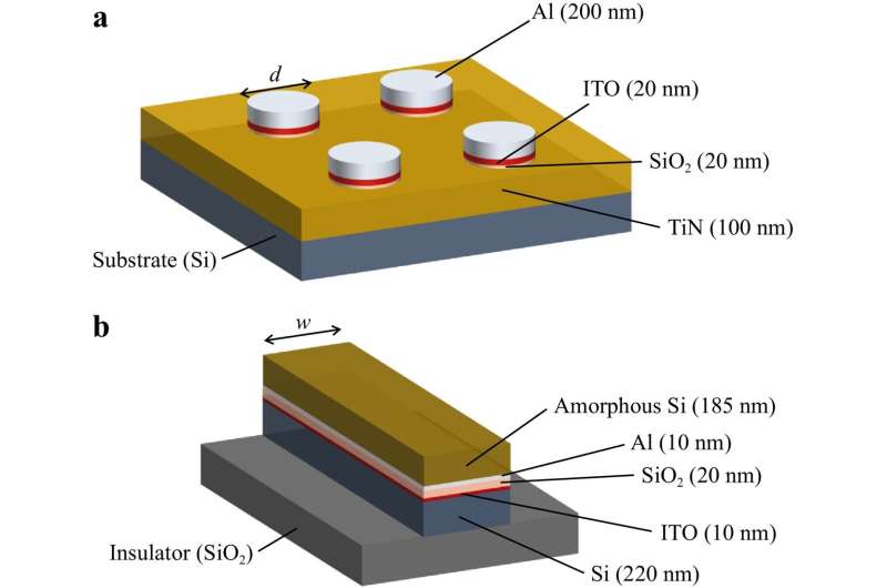
In their paper published in Light: Advanced Manufacturing, researchers from The Edward S. Rogers Sr. Department of Electrical & Computer Engineering at the University of Toronto demonstrated the effectiveness of their new method by fabricating two MIS devices. The first device employed a SiO2/ITO heterostructure grown on thin polycrystalline titanium nitride (poly-TiN) and capped at the ITO side with an aluminum (Al) thin film contact electrode. The second device is an optical waveguide incorporating a semiconductive ITO layer with a SiO2 dielectric spacer implemented on a silicon-on-insulator (SOI) platform.
Dr. Charles Chih-Chin Lin, one of the study's co-authors, commented, "This research marks a significant advancement in the field of plasmonics. We believe that it has the potential to revolutionize the way we design and fabricate photonic devices."
Dr. Swati Rajput, another co-author of the study, added, "The development of CMOS-compatible plasmonic waveguides is a critical step towards realizing the next generation of optical devices. Our research provides a promising pathway towards achieving this goal."
Sherif Nasif, a third co-author of the study, remarked, "We are thrilled about the potential applications of this technology. We envision a future where plasmonic waveguides play a pivotal role in a wide range of industries, including telecommunications, health care, and manufacturing."
The researcher's new method overcomes the challenge of integrating plasmonic structures into CMOS technology utilizing SiO2/ITO heterointerfaces. ITO is a transparent conductive oxide that is compatible with CMOS technology. SiO2 is a dielectric material that is commonly used in CMOS devices. The SiO2/ITO heterointerface provides a strong electric field that can be used to modulate light propagation in the plasmonic waveguide.
Both devices exhibited excellent performance. The light-modulating waveguide had an extinction ratio (ER) greater than 1 dB/µm and an insertion loss (IL) of less than 0.13 dB/µm for a 10 µm waveguide length. The second device achieved amplitude, phase, or 4-quadrature amplitude modulation.
The team's research is a significant step forward in developing CMOS-compatible plasmonic waveguides. Their new method will potentially make plasmonic waveguides more practical for a plethora of applications.
"Our results demonstrate the potential of SiO2/ITO heterointerfaces for CMOS-compatible plasmonic waveguide modulation," said Dr. Alfaraj. "We believe this technology could be used to develop a new generation of photonic devices."
"We are very excited about the potential of this new technology," said Dr. Helmy.
More information: Nasir Alfaraj et al, Facile integration of electro-optic SiO2/ITO heterointerfaces in MIS structures for CMOS-compatible plasmonic waveguide modulation, Light: Advanced Manufacturing (2023). DOI: 10.37188/lam.2023.038
Provided by TranSpread


