August 9, 2023 report
This article has been reviewed according to Science X's editorial process and policies. Editors have highlighted the following attributes while ensuring the content's credibility:
fact-checked
peer-reviewed publication
trusted source
proofread
A first-of-its-kind chip features both a laser and waveguide to create a photonic integrated circuit

A team of computer and electrical engineers at the University of California, Santa Barbara, working with several colleagues from California Institute of Technology and another pair from Anello Photonics has developed a first-of-its-kind chip that hosts both a laser and a photonic wave guide. In their paper published in the journal Nature, the group describes how they made the chip and how well it worked when tested.
With the advent of the integrated circuit, scientists learned to put transistors, diodes and other components on a single chip, greatly increasing their potential. Over the past several years, researchers working with photonics have hoped to achieve the same feat. Those in the field have suggested that the development of an analogous photonic chip could lead to more precise experiments with atomic clocks and could also be used in quantum applications. It would also reduce the need for huge optical tables.
For such a chip to work, it would have to house both a laser and a photonic waveguide. To that end, engineers had developed insert isolators to prevent reflections that lead to instabilities that occur without them. Unfortunately, such an approach requires the use of magnetics, which leads to problems in production. In this new effort, the research team found a way to overcome these problems to create the first truly usable combined chip.
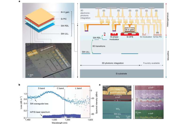
To create the chip, the researchers started by putting an ultralow-loss silicon nitride waveguide on a silicon substrate. They then covered the waveguide with multiple applications of silicon over which they mounted a low-noise indium phosphate laser. By separating the two components, the team prevented damage to the waveguide during etching.
The team notes that separating the two components also required the use of a redistribution layer made of silicon nitride to allow for interactions between the two components via evanescent fields. The distance created between the two components by the silicon layers minimizes interference.
The researchers tested their chip by first measuring its noise levels. Finding them satisfactory, they then used it to create a tunable microwave frequency generator. They describe their chip as "a critical step towards complex systems and networks on silicon."
More information: Chao Xiang et al, 3D integration enables ultralow-noise isolator-free lasers in silicon photonics, Nature (2023). DOI: 10.1038/s41586-023-06251-w
Journal information: Nature
© 2023 Science X Network


