Photon-controlled diode: An optoelectronic device with a new signal processing behavior

A photodetector is a kind of optoelectronic device that can detect optical signals and convert them into electrical signals. These devices include photodiodes, phototransistors and photoconductors.
Although there are many types of photodetectors with different mechanisms and structures, depending on their electrical output characteristics before and after illumination, the representative behavior can be summarized as a limited number: the output current of a photodiode changes from a rectified to a fully-on state after illumination, while the output current of a photoconductor or a phototransistor changes from a fully-off to a fully-on state.
From the perspective of the signal change behavior, there should be a new device that changes the output current from fully-off to rectified state, and may play a key role in future optoelectronic systems, such as optical logic, high-precision imaging and information processing. For instance, rectification controlled by light can avoid the crosstalk issue of photodetector arrays without using selectors, thereby helping to further improve the integration of the array.
Recently, in a paper published in National Science Review, Dong-Ming Sun Group of the Institute of Metal Research, Chinese Academy of Sciences proposes a new device called a photon-controlled diode which can change the output current from a fully-off state to a rectified state after illumination, leading to an anti-crosstalk photomemory array without using any selectors.
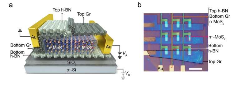
The scientists used a lateral n/n− molybdenum disulfide (MoS2) junction as a channel, graphene as contact electrodes and hexagonal boron nitride (h-BN) as a photogating layer material to fabricate the photon-controlled diode, which is essentially a n/n− MoS2 junction inserted between two graphene/MoS2 Schottky junctions at the cathode and the anode.
Controlled by light, the Schottky junctions suppress or permit the rectification behavior of the n/n− junction, so that the output current of the photon-controlled diode can change from fully-off to rectified state. The light-to-dark rectification ratio can be as high as more than 106. As a photodetector, its responsivity exceeds 105 A/W, while by increasing the thickness of the photogating layer, the behavior of the device changes to a multifunctional photomemory with the highest nonvolatile responsivity of 4.8×10⁷ A/W and the longest retention time of 6.5 × 10⁶ s reported so far.
Using the photon-controlled diodes as pixel units, a 3×3 photomemory array is fabricated without using any selectors, showing no crosstalk as well as functions of wavelength and power density selectivity. This work paves the way for the development of future high-integration, low-power and intelligent optoelectronic systems.
More information: Shun Feng et al, A photon-controlled diode with a new signal-processing behavior, National Science Review (2022). DOI: 10.1093/nsr/nwac088
Provided by Science China Press


