December 20, 2021 feature
Exploring factors impacting the sensitivity of amorphous oxide semiconductors to externally induced impurities

In recent years, electronics engineers have been trying to broaden the pool of available semiconducting materials, to enable the development of a wider range of devices. One emerging class of semiconductors are amorphous oxide semiconductors (AOSs), which are semiconductors based on oxides of post-transition metals.
These semiconductors can have several advantageous properties, including the ability to be deposited at low temperatures and across large surfaces, as well as a high flexibility and carrier mobility. These advantages would make them particularly suitable for creating low-cost and large-area devices, such flat-screen displays. Nonetheless, so far these materials have had a series of limitations that prevented them from replacing existing polycrystalline silicon technologies on a large scale.
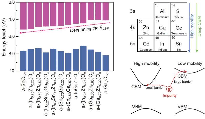
Researchers at Tokyo Institute of Technology have recently carried out a study aimed at examining some of these limitations more closely. Their paper, published in Nature Electronics, shows that the sensitivity of AOSs to externally introduced impurities and defects is highly dependent on the location of the so-called conduction-band minimum (CBM).
"In 2004, the first amorphous oxide semiconductor (AOS), IGZO, TFT was demonstrated by our institute, in a project led by Prof. Hosono," Jungwan Kim, one of the researchers who carried out the study, told Phys.org. "Since I joined the current group in 2012, I mainly studied the electronic structure, doping mechanism and defects of AOSs. In 2017, in a study on amorphous gallium oxide (a-Ga2Ox), we found that energy levels and the relevant doping abilities of AOSs significantly differ according to their chemical composition."
Based on their previous findings, Kim and his colleagues concluded that the number of donors (e.g., oxygen vacancy defects or hydrogens) in AOSs does not impact the carrier density. For instance, a-Ga2Ox film possesses the carrier density of only 1015 cm-3, even it contains same number of hydrogens as the amorphous InSnZnO (a-ITZO), which has a carrier density of 1020 cm-3. These observations inspired the researchers to examine the correlation between the electronic structure of AOSs and their doping ability further.
"Our explorations ultimately led to the achievement outlined in Nature Electronics," Kim explained. "Most notably, we found that a charge transfer occurs between AOSs and unintended impurities and the charge transfer is strongly governed by the energy levels of the materials."
The researchers found that the electron mobility of AOSs can be tuned by altering their chemical composition. In their experiments, Kim and his colleagues used ultraviolet photoemission spectroscopy (UPS) to determine the energy levels in an AOS, for instance identifying the conduction band minimum (CBM) and valence band maximum (VBM) levels.
"In general, as the indium (In) or Tin (Sn) content increases, the electron mobility increases," Kim explained. "The mobility-stability can thus be easily compared by investigating the different chemical composition systems."
The recent experiments carried out by Kim and his colleagues showed that a charge transfer occurs between AOSs and unintended, externally introduced impurities. Moreover, this charge transfer appears to be strongly influenced by the materials' energy levels.
Typically, it is rare and unadvisable for impurities to remain in materials that are used to fabricate electronics. However, due to their low temperature processes, which are also advantageous, AOSs are particularly sensitive to impurities.
"This aspect of AOSs sets them apart from conventional Si-based electronics," Kim said.
"I feel that we are too used to conventional Si-based electronics. Much more different viewpoints should be prepared for low-temperature electronics. In this case, the discovered impurity was CO-related impurities which donate electrons to AOSs under the negative gate bias stress condition."
CO-related impurities are a type of impurities that can be easily avoided and prevented when fabricating electronics on a large-scale. The recent findings gathered by this team of researchers thus suggest that attaining better performing thin-film transistors (TFTs) based on AOSs could be possible when using advanced manufacturing equipment.
Nonetheless, the team suspects that there might be additional impurities and defects affecting the charge transfer of AOSs. They thus plan to conduct further studies examining the impact of different types of impurities on these materials' properties and performance.
"Oxide TFT manufacturing processes, what kinds of impurities are generated and how much of these impurities are incorporated in the AOSs must be thoroughly investigated," Kim said. "For more applications such as logic circuits, memory, fully transparent electronics, there remains many challenging tasks. In our next studies, we will focus on the following topics: origin of dopant in AOSs, mobility limitation in AOSs, etc."
More information: Yu-Shien Shiah et al, Mobility–stability trade-off in oxide thin-film transistors, Nature Electronics (2021). DOI: 10.1038/s41928-021-00671-0
Room-temperature fabrication of transparent flexible thin-film transistors using amorphous oxide semiconductors. Nature(2004). DOI: 10.1038/nature03090.
Conversion of an ultra-wide bandgap amorphous oxide insulator to a semiconductor. NPG Asia Materials(2017). DOI: 10.1038/am.2017.20.
Journal information: Nature Electronics , Nature
© 2021 Science X Network


