A survey on optical memory and optical RAM technologies

Over the past decades, 'storing light' has appeared as a rather controversial concept, given that a photon's inherent nature hinders its spatial confinement. The first research efforts in demonstrating optical memory functionality started as a fascinating experimental exercise, and two decades later the remarkable achievements of integrated optical memories and optical random access memories (RAMs) introduced a new roadmap for light-based information storage that can offer fast access times, high bandwidth and seamless cooperation with optical interconnect lines.
In a new paper published in Light Science & Applications, a team of three Greek researchers, Dr. Theoni Alexoudi and Prof. Nikos Pleros from Department of Informatics of Aristotle University of Thessaloniki in Greece together with their co-worker Prof. George T. Kanellos from Bristol University in the UK have evaluated the progress witnessed in the optical memory domain over the past 25 years.
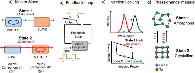
Their article provides a thorough analysis on the state-of-the-art integrated optical memory technologies and optical RAMs, shedding light on the physical mechanisms behind demonstrated optical memory devices. In the same analysis, optical memory implementations are also being classified and evaluated via their performance metrics highlighting the benefits of different optical technologies. The authors provide a comprehensive guide for the transition from elementary optical memory units towards advanced memory functionalities such as optical RAM operation, and report recent achievements towards this direction. Finally, an analysis is presented for the next steps that optical memory technologies must undertake to release a viable and practical alternative memory roadmap.
These scientists summarize some of the key-findings of their review study:

"Optical memories have gradually penetrated into multiple application sectors that include processing, routing, and computing however, modern memory applications call for advanced memory schemes with random access functionality on top of the simple storage mechanism."
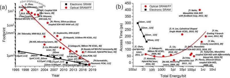
"Optical memories have witnessed an impressive progress in terms of footprint. Their footprint reduced by 12-orders-of-magnitude going from m2 to μm2 during the last 20 years while at the same time electronic counterparts were reduced only by 3 orders-of-magnitude," they add.
"Optical memory integration roadmap has to be shaped around a high-yield and low-cost fabrication technology allowing for dense optical memory architectures to arrive at scales, complexities and cost-efficiencies similar to those of their electronic counterparts." the scientist conclude.
More information: Theoni Alexoudi et al, Optical RAM and integrated optical memories: a survey, Light: Science & Applications (2020). DOI: 10.1038/s41377-020-0325-9
Journal information: Light: Science & Applications
Provided by Chinese Academy of Sciences


