Microwave-based test method can help keep 3-D chip designers' eyes open

Researchers at the National Institute of Standards and Technology (NIST) have invented a new approach to testing multilayered, three-dimensional computer chips that are now appearing in some of the latest consumer devices. The new method may be the answer the semiconductor industry needs to quickly assess the reliability of this relatively new chip construction model, which stacks layers of flat circuitry atop one another like floors in a building to help make chips ever-faster and packed with features.
The approach overcomes the limitation of conventional chip-testing methods on the so-called 3-D chips, which include many thin horizontal "floors" connected to one another by vertical pathways called through-substrate vias, or TSVs. These TSVs are essential to the operation of 3-D chips, which have become commercially viable only in the past few years after decades of sustained development effort by the industry.
With NIST's new testing method, chip designers may have a better way to minimize the effects of "electromigration," a perennial cause of chip failure rooted in the wear and tear that relentless streams of flowing electrons inflict upon the fragile circuitry that carries them. The NIST approach could give designers a quicker way to explore the performance of chip materials in advance, thereby providing more, and almost real-time, insight into what materials will best serve in a 3-D chip.
"Our work shows it may be possible to spot microscopic failures faster," said NIST's Yaw Obeng, research chemist and the leader of the Metrology for Emerging Integrated Systems project. "Instead of waiting for months, we can see in days or hours when it's going to happen. You can run our tests during the material selection phase to see how processing will affect the end product. If you can't see it, you might make the wrong decision."
If a 3-D chip were a high-rise building, TSVs would be its elevators. They help 3-D chips do three essential things: Speed up, shrink down and cool off. By allowing elements on different floors to communicate with each other, signals no longer need to travel all the way across a comparatively sprawling 2-D chip, meaning calculations go faster and electrons heat up far less conducting material as they move.
Along with these advantages, TSVs also carry one drawback: Their reliability is hard to test with the conventional method, which involves passing direct current through the conductor and waiting for its resistance to change. It is very time-consuming, requiring weeks or even months to show results. The chip industry needs a new metrology approach that is quick and realistic, and that would reveal the impact on the high-speed signal that actually runs through the conductors.
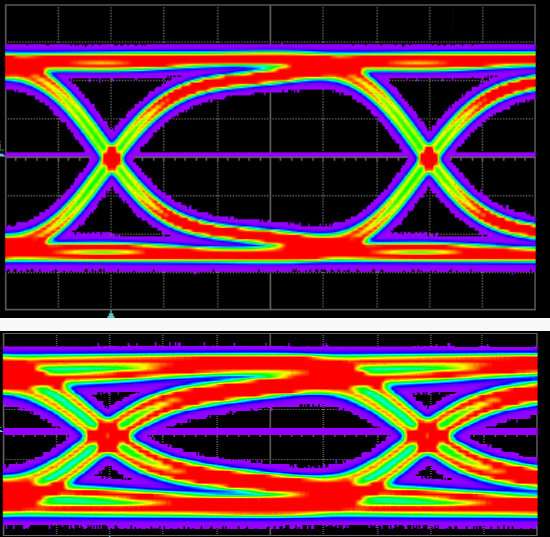
The new NIST testing method sends microwaves through the material and measures changes in both the amount and quality of the signal. Their testing setup, which simulates real-world conditions, repeatedly heats and cools the material, causing it to develop flaws, and over time, the microwave signal decreases in strength and decays from a clean, square-shaped wave to one that is noticeably distorted.
Using microwaves brings multiple benefits. Perhaps chief among them is how rapidly the method provides information about a device's reliability, in the actual device of interest, long before it actually fails—a possibility unavailable with the resistance-based approach.
"Before failure comes what we call a 'quiescent period' when the beginnings of defects are blowing around through the material, like seeds in the wind," Obeng said. "The microwaves show this process happening. If you just watch the material with resistance, you don't see this, it's either alive or dead."
Microwaves could reveal information about defects as quickly as three days after testing begins, while conventional tests can take months.
Obeng estimates this method could be fully implemented by industry within a few years, and could provide valuable insights.
"This approach would give materials designers insight into what materials to use in chips and how to build them," he said. "Making the right decisions can result in an end product that's more stable and reliable. This will give them more information to make those decisions."
More information: Christopher E. Sunday et al, Microwave evaluation of electromigration susceptibility in advanced interconnects, Journal of Applied Physics (2017). DOI: 10.1063/1.4992135
Journal information: Journal of Applied Physics
Provided by National Institute of Standards and Technology


