March 17, 2016 report
Researchers use electron microscope to reveal how semiconductor nanowires grow
(Phys.org)—A team of researchers with members from Sweden, the U.K. and the U.S. has used a transmission electron microscope to discover the secrets behind how nanowires used to make semiconductors grow. In their paper published in the journal Nature, the team describes their microscopic study of gallium arsenide nanowires during their growth phase and what they learned about the process. Anna Fontcuberta i Morral with École Polytechnique Fédérale de Lausanne in Switzerland offers a News & Views Perspective piece on the work done by the team in the same journal issue outlining the process used and explaining what the results will mean for advances in electronics, photonics and quantum information research efforts.
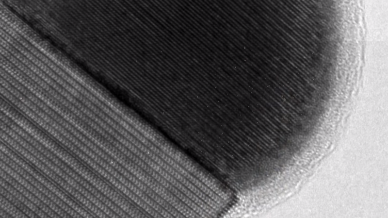
Scientists have discovered many useful properties of crystals leading to the development of many modern products, such as computers and photonic devices. Such devices depend on an ability to grow crystals in ways that suit particular needs. But, as Fontcuberta i Morral notes, a complete understanding of what occurs during the initial stages of crystal growth is holding back the development of a wider range of products. In this new effort, the researchers sought to learn more about polytypism—where a compound has the ability to exist as various crystal forms with differences only in their bilayer structure—by taking a very close look at the initial stages of gallium arsenide nanowire formation during the vapor–liquid–solid method. They report that their observations revealed that new bilayers formed at the triple-phase line, resulting in a flat layer at the top, but when the liquid-metal droplet used as a catalyst grew to a certain size, an edge appeared which altered the growth of the crystal—bilayers suddenly formed faster and the edge began to oscillate.
The researchers suggest that their observations revealed that droplet size directly impacted the contact angle and the morphology of the liquid-solid interface. They noted also that angles close to 90° typically resulted in nucleation of bilayers, whereas smaller angles typically led to suppression of nucleation of bilayers allowing for the formation of zinc-blende structures.
Fontcuberta i Morral suggests the findings by the team provide a new pathway towards crystal-phase design, allowing for engineers to select the crystal phase they desire for particular applications.
More information: Daniel Jacobsson et al. Interface dynamics and crystal phase switching in GaAs nanowires, Nature (2016). DOI: 10.1038/nature17148
Abstract
Controlled formation of non-equilibrium crystal structures is one of the most important challenges in crystal growth. Catalytically grown nanowires are ideal systems for studying the fundamental physics of phase selection, and could lead to new electronic applications based on the engineering of crystal phases. Here we image gallium arsenide (GaAs) nanowires during growth as they switch between phases as a result of varying growth conditions. We find clear differences between the growth dynamics of the phases, including differences in interface morphology, step flow and catalyst geometry. We explain these differences, and the phase selection, using a model that relates the catalyst volume, the contact angle at the trijunction (the point at which solid, liquid and vapour meet) and the nucleation site of each new layer of GaAs. This model allows us to predict the conditions under which each phase should be observed, and use these predictions to design GaAs heterostructures. These results could apply to phase selection in other nanowire systems.
Journal information: Nature
© 2016 Phys.org


