Towards the development of a new evaluation method of semiconductors by using terahertz waves

Wide-gap semiconductors such as gallium nitride (GaN) are widely used for optical devices such as blue LED and are also anticipated as materials for next-generation energy saving power devices and solar cells. However, the quality of GaN crystals does not come up to that of conventional semiconductor materials such as silicon (Si) and this prevents GaN from being used for power devices.
For that reason, the establishment of technology for producing high-quality crystals with fewer defects and rearrangement is expected, and the development of a new evaluation technology is crucial.
A group of researchers led by Iwao Kawayama, an associate professor of the Institute of Laser Engineering at Osaka University, in cooperation with Screen Holdings Co., Ltd., succeeded in visualizing changes in defect density on the surface of GaN through the laser terahertz emission microscope (LTEM) which measures THz waves generated by laser emission. This group's discovery shows that LTEM is useful as a new method for evaluating the quality of wide-gap semiconductors and it is also expected that LTEM will bring a breakthrough in the development of next-generation optical devices, super high frequency devices, and energy devices.
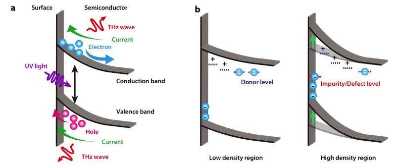
The group examined the intensity distribution of THz generated by radiating ultraviolet femtosecond laser pulses on the surface of GaN crystal through LTEM. As a result, it was found that there were regions with high intensity of THz emission and ones with low intensity of THz emission.
Additionally, when the LTEM image was compared with the image obtained through photoluminescence (PL) using a conventional method, it was found that there was a strong correlation between the distribution of emission intensity due to lattice defects and the intensity distribution of THz wave emission.
Furthermore, from results measurement through modification of excited lasers, it was confirmed that THz emission needs excitation light with larger energy than the band gap energy.
This research was featured in the electronic version of Scientific Reports on September 9, 2015.
More information: "Visualization of GaN surface potential using terahertz emission enhanced by local defects." Scientific Reports 5, 13860 (2015) DOI: 10.1038/srep13860
Journal information: Scientific Reports
Provided by Osaka University


