Diode a few atoms thick shows surprising quantum effect

A quantum mechanical transport phenomenon demonstrated for the first time in synthetic, atomically-thin layered material at room temperature could lead to novel nanoelectronic circuits and devices, according to researchers at Penn State and three other U.S. and international universities.
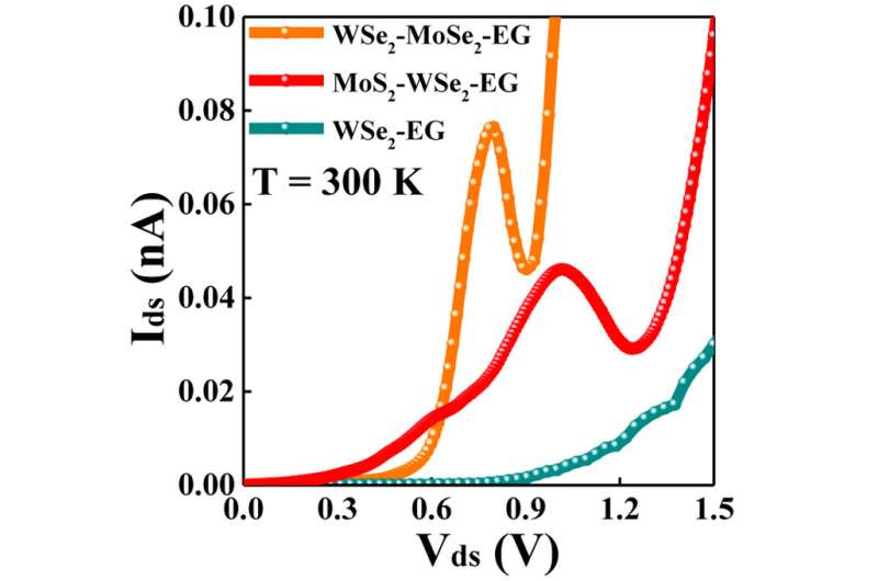
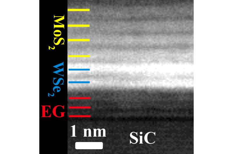
The quantum transport effect, called negative differential resistance (NDR), was observed when a voltage was applied to structures made of one-atom-thick layers of several layered materials known as van der Waals materials. The three-part structures consist of a base of graphene followed by atomic layers of either molybdenum disulfide (MoS2), molybdenum diselenide (MoSe2), or tungsten diselenide (WSe2).
NDR is a phenomenon in which the wave nature of electrons allows them to tunnel through any material with varying resistance. The potential of NDR lies in low voltage electronic circuits that could be operated at high frequency.
"Theory suggests that stacking two-dimensional layers of different materials one atop the other can lead to new materials with new phenomena," said Joshua Robinson, a Penn State assistant professor of materials science and engineering whose student, Yu-Chuan Lin, is first author on a paper appearing online today, June 19, in the journal Nature Communications. The paper is titled "Atomically Thin Resonant Tunnel Diodes Built from Synthetic van der Waals Heterostructures."
Achieving NDR in a resonant tunneling diode at room temperature requires nearly perfect interfaces, which are possible using direct growth techniques, in this case oxide vaporization of molybdenum oxide in the presence of sulfur vapor to make the MoS2 layer, and metal organic chemical vapor deposition to make the WSe2 and MoSe2.

"This is the first time these vertical heterostructures have been grown like this," Robinson said. "People typically use exfoliated materials that they stack, but it has been extremely difficult to see this phenomenon with exfoliated layers, because the interfaces are not clean. With direct growth we get pristine interfaces where we see this phenomenon every time."
What caught Lin and Robinson's attention was a sharp peak and valley in their electrical measurements where there would normally be a regular upward slope. Any unexpected phenomenon, if it is repeatable, is of interest, Robinson said. To explain their results, they consulted an expert in nanoscale electronic devices, Suman Datta, who told them they were seeing a 2D version of a resonant tunneling diode, a quantum mechanical device that operates at low power.
"Resonant tunnel diodes are important circuit components," said Datta, a coauthor on the paper and Penn State professor of electrical engineering. "Resonant tunneling diodes with NDR can be used to build high frequency oscillators. What this means is we have built the world's thinnest resonant tunneling diode, and it operates at room temperature."
Coauthor Robert Wallace of the University of Texas at Dallas said this collaborative work represents an important achievement in the realization of useful 2D integrated circuits.
"The ability to observe the resonant behavior at room temperature with synthesized 2D materials rather than exfoliated, stacked flakes is exciting as it points toward the possibilities for scalable device fabrication methods that are more compatible with industrial interests. The challenge we now must address includes improving the grown 2D materials further and obtaining better performance for future device applications," Wallace said.
The UT-Dallas coauthors provided the detailed atomic resolution materials characterization for the resonant tunneling diodes discovered at Penn State.
Datta credits a theoretical understanding of the electron transport in the 2D layered materials to his post-doctoral researcher Ram Krishna Ghosh, whose calculations show close correspondence to the experimental results. Datta cautioned that the new resonant tunnel diode is just one element in a circuit and the next step will require building and integrating the other circuit elements, such as transistors, in 2D.
"The take home message," he said, "is that this gives us a nugget that we as device and circuit people can start playing around with and build useful circuits for 2D electronics."
More information: Atomically thin resonant tunnel diodes built from synthetic van der Waals heterostructures. Nature Communications, 2015; 6: 7311. DOI: 10.1038/ncomms8311
Journal information: Nature Communications
Provided by Pennsylvania State University


