An electrical wire a few atoms wide
EPFL researchers showed it is possible to create an electrical channel a few atoms wide within two-dimensional insulating materials. Their simulations open new perspectives for the production of new electronic and photovoltaic devices.
In the world of the infinitely small, unexpected phenomena can occur at the interface between two materials when they are artificially combined. At EPFL scientists have shown that it is possible to generate a conducting channel with a width of a few atoms in the contact zone between different sheets of insulating materials. This work, just published in Nature Communications, could enable the creation not only of new micro- and nanoelectronic devices but also of a new kind of solar cell.
Two-dimensional materials
To generate these tiny conducting channels, researchers studied two-dimensional materials, that is to say sheets of material a few atoms thick, sometimes only consisting of a single layer of atoms.
Like graphene, these materials are composed of atoms arranged in a hexagonal structure, similar to the cells found in beehives. The difference is that while graphene is conductive and only composed of carbon atoms, the two-dimensional materials mentioned in the study are insulating and are composed of different elements.
Among many possibilities, researchers considered boron nitride (BN), which is composed of two kinds of atoms. In its natural state, a "sheet" of boron nitride acts as an insulator and therefore cannot conduct electric current. However, the technique, after a slight chemical modification, allows researchers to develop "leads" for conductive electrons.
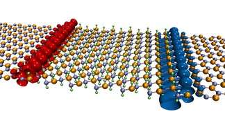
A proton sandwich
The fabrication of the electrical channel is a two-step operation. It is made by fixing a proton (i.e., an hydrogen atom) on a sheet of boron nitride above each boron atom (B) and one below each nitrogen atom (N). Thus sandwiched between the hydrogen atoms, the "decorated" boron nitride sheet generates a conductive channel a few atoms wide when it is placed in contact with a "pristine" sheet of BN. The new "wire" located at the interface between the two sheets enables precise control of the circulation of the electrons when tension is applied. "Taken separately, the chemically modified sheet and the blank sheet are not conductive," says Giovanni Pizzi, co-author of the study. "It is only by combining one with the other that the channel appears."
Potential applications associated with these simulations are numerous. The new conductive "wires" could particularly serve to develop more compact and powerful micro- and nanoelectronic devices. "The 'wires' produced by traditional lithography don't fall below twenty nanometers, which means at least one hundred atoms," says Giovanni Pizzi. "A few atoms wide, our wire could connect the different processors of a nanochip by taking far less space than current wires."
A new model of solar cell
Applications related to these tiny conductive channels could also include the creation of a new kind of ultra-thin and flexible solar cell.
When the material patterned with channels is subjected to sunlight, electrons present in the insulating part move toward the conductive pathways. "To obtain an electric current, it then suffices simply to connect the channels," explains Marco Gibertini, who also co-authored the study.
Towards experimental tests
EPFL researchers now hope their simulation work attracts the attention of specialists in the experimental area to conduct tests in real-life settings. "In our study we provide a simple calculation that researchers can perform to see if a given material, after chemical modification, will form these tiny wires," says Marco Gibertini. "Our idea relies on previous results on 3D materials. We have also intentionally investigated existing experimental materials and techniques. This should facilitate experimental tests," he adds.
More information: "Engineering polar discontinuities in honeycomb lattices." Nature Communications 5, Article number: 5157 DOI: 10.1038/ncomms6157
Journal information: Nature Communications
Provided by Ecole Polytechnique Federale de Lausanne


