Practical chip-level optical interconnects

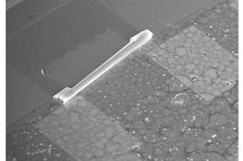
In efforts toward creating practical chip-level optical interconnects, researchers in Canada present the first nanoscale tube based photodetector, compatible with silicon platform integration.
The difficulties of building on sand
Nanoscale photodetectors are important for the future of optical computing and have potential for ultra-high-speed operation and very low power consumption. For practical chip-level optical interconnects, it is also important that photodetectors can be directly integrated with other electronic components on a silicon platform.
Silicon is not a suitable material for photodetection in optical communication owing to its relatively large bandgap. Devices based on other semiconductors like germanium and III-V compounds are well known, with good performances having been demonstrated in the optical communication wavelength range (1.3 µm-1.55 µm).
However, their direct integration on Si substrate generally leads to very large densities of dislocations in the device active region, because of the large lattice mismatch and differences in the thermal expansion coefficients. This results in device performances that are impractically poor. Flip chip integration and bonding techniques have also been used to transfer active III-V membrane devices onto silicon, but this is a high-cost, time consuming process.
More recently, improved results have been obtained by growing 'self-organised' III-V compound quantum dot (QD) structures directly on silicon. Self-organised QDs are defect-free nanoscale islands spontaneously formed during epitaxial growth when the grown film thickness exceeds a critical value.
QDs are nearly free of dislocations and can suppress the propagation of defects during device operation under harsh conditions, giving long term reliability. In addition, the operation wavelength can be readily tuned by engineering the size and composition of the grown QDs.

On a roll
The team from McGill University, Montreal, have previously demonstrated that nanoscale QD tube devices can be grown and transferred onto virtually any substrate. This gives a viable approach for integration of high performance III-V based nanoscale photonic devices with silicon electronics, as their performance does not suffer from lattice and thermal mismatches between the III-V material and the Si substrate. The team are now reporting the first demonstration of a nanoscale tube based photodetector.
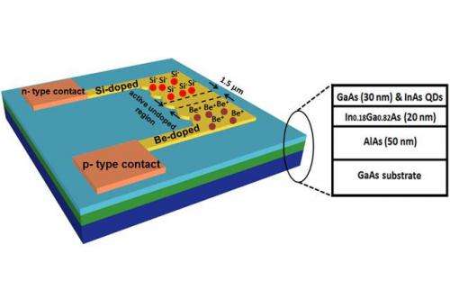
The microtube structure of the photodetector is produced by rolling-up an InAs/GaAs QD nanomembrane. The rolling is driven by a coherent strain that is intentionally introduced in the QD heterostructures during growth by molecular beam epitaxy. By selectively etching the underlying AlAs sacrificial layer, the strained QD heterostructure rolls up to form a tubular cavity under strain relaxation.
"The InAs QDs embedded in the tube centre region act as the active material of the photodetector. Subsequently, we defined a pin diode along the tube axial dimension using a two-step selective area ion-implantation process. By exposing the active region of the microtube to 1064 nm and thus exciting the InAs QDs within the tube structure, we could clearly measure the induced photocurrent," explained team member Prof. Zetian Mi.
"The major challenge to overcome was to define a functional ppin junction along the rolled-up tube axial dimension. To do this, we have optimised the fabrication steps, including a two-step selective area ion implantation process, in order to make rolled-up tube devices with electrical contacts formed on the tubular surfaces. Moreover, we have optimised the annealing and etching conditions to achieve rolled-up devices that are virtually free of defects for high efficiency photodetection."
In addition to its silicon integration capability, in this design the light absorption length and carrier transport are along separate directions, allowing separate optimisation of the photodetector's efficiency and speed. The use of a microtube optical cavity can also significantly enhance light absorption at desired wavelengths by coupling to the cavity modes.
In the tube
The McGill researchers are now working to further improve the external quantum efficiency of the photodetector design by using multiple QD structures and optimising tube diameter to enhance efficiency at the operation wavelength through resonance.
They are also applying their methods to other kinds of device, including high speed electrically injected nanoscale tube lasers and their integration with other electronic and optoelectronic components; working towards the goal of achieving chip-level optical interconnects using III-V nanoscale devices on silicon.
Looking beyond this, Mi said: "We have also been working on nanoscale photonic and electronic materials and devices, including the epitaxial growth and fundamental properties of QDs and nanowires and high efficiency LEDs, lasers, and solar fuel devices and systems. We expect that this area will quickly evolve from lab innovation to commercialisation. Such tube devices have been widely studied for applications other than optical interconnects, including biosensors, energy harvesting, microfluidics, and MEMS/NEMS."
More information: "Nanoscale rolled-up InAs quantum dot tube photodetector." M.H.T. Dastjerdi, Z. Mi. Electronics Letters, Volume 50, Issue 9, 24 April 2014, p. 680 – 682. DOI: 10.1049/el.2013.4070 , Print ISSN 0013-5194, Online ISSN 1350-911X
Journal information: Electronics Letters
Provided by Institution of Engineering and Technology
This story is published courtesy of Electronics Letters. For additional Electronics Letters news and features visit theiet.org/eletters


